|
The Journal of The Institute of Circuit Technology Welcome to our latest Technical Journal. The journal is published quarterly and distributed to Industry Experts. We invite you to join our mailing list and be part of our aim of disseminating and publishing technical and training information for the greater benefit of our industry. This is a complimentary subscription with no commitment. Subscribe to The Journal. The next issue will be sent to you in July 2023 |
||
| |
||
|
The Journal of |
| Section 1 | Editors Introduction |
|
Richard Wood-Roe |
In this issue of The Journal we have included a paper from Don Ball of Chemcut, explaining the practical aspects of etching copper for HDI applications. There is an absorbing overview of thermal management in high performance RF and microwave pcb's from John Priday of Teledyne. There is a paper describing a novel 2-layer solder mask for extreme applications from Ying Hsuan Chou of Taiyo. We also have an unusual paper from Radu Burlica, from Romania, on ambient plasma treatment for adhesion promotion for use in printed electronics. We now have a video gallery of Happy Holden's valuable contribution to our series of Technical Webinars. This can be accessed from section 7 of this journal as well as links on our website. In section 9 we give details of our members who have been awarded Honorary Fellow gradings for their contribution to the PCB industry. I am grateful to Pete Starkey for his write up of the recent ICT AGM and evening seminar that was held in Meriden, West Midlands. Finally the industry news section highlights the activity of some of our Corporate Members. |
| Go back to Contents |

| Section 2 | Calendar of Events | |
Bill Wilkie |
2023 |
Details |
| March 7th | ICT AGM and Spring Seminar at Meriden. Council Meeting – Starts at 12 noon, Fab Group Meeting starts at 14:30, AGM/Seminar starts at 18:00 – to be followed by a buffet. Manor Hotel Room Rate - £100/night B&B at ICT Rates |
|
| April 24-27th | Annual Foundation Course, Chester It is Annual Foundation Course time again and we are now in the 43rd year of this venerable Institution. Only three people have ever been in charge of the course, Geoff Paterson, who was the Technical Manager of Bepi Electronics and a Course founder, Lawson Lightfoot and Bill Wilkie. Details of this years' course can be found here. Read more... |
|
| June 6th | ICT Annual Symposium at the National Motorcycle Museum at the NCC, Birmingham | |
| Go back to Contents | ||

| Section 3 |
Practical Aspects of Selective Etching for High Density Interconnect Editors Note: This paper is a few years old now. It has been included as it is still very relevant to today's manufacturing challenges. |
|
Don Ball |
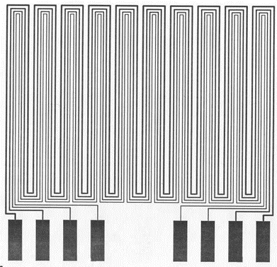
1. Introduction The fully subtractive etching process is still the most economical and fastest way to produce large numbers of printed circuit boards but it has its limitations. First and foremost is the fact that the etch process etches sideways as well as down at a ratio of an approximately 1 unit increase in the width of a space to every 3 or 4 units down, depending on the etchant and etching conditions. This means there is a limit to the thickness of the copper foil in relation to the widths of the lines and spaces for HDI. Presently the practical limits for lines and spaces are 75µm (3 mil) lines and spaces in 35µm (1 oz.) foil, 50µm (2 mil) lines and spaces in 18µm (1/2 oz.) foil and 25µm (1 mil) lines and spaces in 9µm (1/4 oz.) or 5µm (1/8 oz.) foil. So far the seemingly insatiable demand for smaller, lighter electronic devices with more and more capabilities built in have been met, in part, by decreasing the size of the lines and spaces on the interconnect boards and using thinner foils to accommodate the narrower lines and spaces. However, thinner foils also limit the amount of amperage that can go through those high density interconnects. In the past year or so we have begun to get requests to look at the feasibility for the near future of production based on 50µm lines and spaces in 35µm foil and 25µm lines and spaces in 18µm foil using 30µm (1.2 mil) dry film. This initiated some internal tests and it is the results of these tests, which include some insights on what the problems with HDI etching really are, some proposed solutions for these problems, and tests of the proposed solutions, that are presented here. The conclusion reached is that the proposed objectives are possible but attaining them, especially in a production environment, will be extremely difficult. Since almost all of our testing in the last several years have been based on the practical limitations expressed above the obvious first step was to run some etch tests with 50µm lines and spaces in 35µm foil and 25µm lines and spaces in 18µm foil to see exactly what we were up against. Figure 1 on the next page shows the layout of one of the test patterns. Each pattern is about one inch square (2.54 cm) and there are 352 of these patterns in a 22x16 grid on a 24” x 18” inch (601mm x 457mm) panel. The multi-‐pitch designation means there are four different line and space combinations within each test pattern. The 1,1,1 means this pattern starts with a 1 mil line and space on the innermost pad and line and space widths increase by one for each subsequent pad up to 4 mils. Therefore we have a 1 mil line, 1 mil space, 2 mil line, 2 mil space, etc. There is a 1.5 mil (37µm) space between the two 25 µm lines where they run side-‐by-‐side. For testing the 50µm lines and spaces on 35µm foil a CATs 2,2,1 multi-‐pitch pattern was used. This is essentially the same layout but starting with a 2 mil line and space increasing in steps of one mil to a 5 mil line. Where the 2 mil lines run side-‐by-‐side the space between them is 2.5 mils (63.5µm).
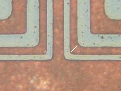
Figure 1 – CATs Test Pattern Etchant Chemistry and Considerations – Cupric chloride is the first choice for etching copper because, with regeneration, it maintains a constant etch rate and generates the least amount of etchant to have to eventually dispose of. Ferric chloride gives a little less undercut and slightly better etch factors when used to etch copper but, when used with copper, it can’t be regenerated so the cost of new etchant and the cost of disposal of the old etchant far outweighs the slight etch quality advantage. Undercut and etch factor have been a concern for many years and we have done extensive testing in the past on different chemistry parameters to minimize undercut and maximize etch factors (to be covered in a little more detail in the next section). The most important factors for cupric chloride etching are specific gravity and free acid content with higher specific gravities and lower free acid contents giving noticeably better results for both undercut and etch factors. The cupric chloride for the tests was run at a specific gravity of 1.330 (36o Be) and a free acid level of 0.8N (29.2 gpl). The results of the 50µm lines and spaces on 35µm copper were encouraging with over 80% yields for the 50µm lines in terms of opens and shorts. This is not great but certainly much higher than expected. The major problem was a very tight window for conveyor speed between over and under etching. It was hoped that similar results could be obtained with the 25µm lines and spaces in the 18µm micron foil since everything was cut by half except for the thickness of the resist. Such was not the case, however, as the test patterns displayed a 100% failure rate due to opens when etched long enough to clean out the 25µm spaces so there were no shorts. The good news was that none of the opens were caused by resist adhesion failures even though the widths at the tops of the lines were as low as 8.2µm (0.33 mils). There were two places where there were always opens. The first were the isolated 25µm lines leading to the pads, which are easy enough to fix with some artwork compensation. The other place was where the 25µm lines took a 90o turn. This was a little puzzling until a little simple geometry was applied as shown in Figure 2 below. Where the 25µm space makes a right angle turn the hypotenuse of the right triangle formed is 35.8µm, giving the etchant a little more space to work in, resulting in a little faster etch rate at this point. By the time the 25µm spaces to either side are etched clean the line at the corner has etched through.
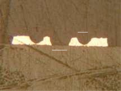
Figure 2 Figure 3 illustrates a little more clearly the difference in etch speed in a 36 to 37µm space as opposed to a 25µm space. This is a cross section showing the 37µm space between adjacent 25µm lines and the 25µm spaces between the adjacent 25µm and 50µm lines after etching. It is quite evident that the 37µm space is nicely cleaned out before the bottom of the 25µm space has even been reached.
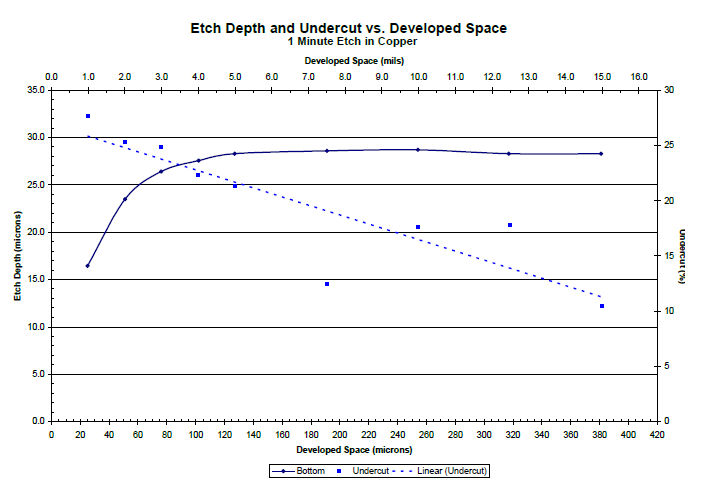
2.4 Etch Rate and Etch Factor vs. Developed Space – Intellectually it is known that, as the space between lines decreases, the time needed to etch them out increases. It was clear after these initial etch tests that the rate of drop off in etch rate was much greater than we anticipated. A simple test was devised to quantify the change in etch rate with decreasing spaces. A test pattern was prepared with 15, 12.5, 10, 7.5, 5, 4, 3, 2 and 1 mil spaces (381, 317, 254, 191, 127, 102, 76, 51 and 25m). The patterns were etched for one minute in cupric chloride and cross sectioned. Measurements were taken of etch depth and etched width across the top of the space. The etch rates were calculated as were the etch factor. In this case the etch factor is the ratio of the increase in width of one side of the space to the depth of etch expressed as a percentage. A higher percentage generally means more undercut (less undercut is more desirable). Figure 4 is a chart showing the results of these tests. The solid line and the left axis are the etch rates and the dashed line and right hand axis are the undercut percentages. These tests were done with a 15µm dry film.
Figure 4 As can be seen, the etch rates in the spaces remains constant until the space gets to 5 mils (125µm). There is a small decrease between 4 and 5 mils (100 and 125µm), a little more decrease between 3 and 4 mils (75 and 100µm) then a large drop off between 2 and 3 mils (50 and 75µm) and an even larger relative drop off between 1 and 2 mil (25 and 50µm) spaces. The fall off in etch rate between the 2 mil (50µm) spaces and 5 mil (125µm) spaces is 17% and the fall off between the 1 mil (25µm) spaces and 5 mil spaces is almost 42%. The difference in etch rates between the 2 mil and 1 mil spaces is almost 30% by itself. It can also be seen that the etch factor percentage also increases as the spaces decrease. This is a little misleading, as the actual increase in the widths of the etched spaces remained fairly constant over the range of spaces in this test; the ratios went up because there was less etch depth in the same amount of time. The best explanation, without getting into such things as fluid viscosity, grain boundary attacks and diffusion layers, for the above phenomena is probably the easiest one. As the depth to be penetrated by the etchant (resist thickness plus foil thickness) increases in relation to the width of the opening available for the etchant to get into, the difficulty of getting fresh etchant to the copper surface and spent etchant away from the copper surface increases and the slowdown in the exchange rate slows the rate of etch. In addition, the above chart shows that the slowdown in etch rate is not linear but exponential. It should also be noted that the fall off in etch rate will be sharper for a thicker resist than the 15µm dry film used in this test and a little shallower for a thinner resist but still substantial. At this point it is possible to get bogged down in all kinds of theoretical explanations and mathematical calculations. Since the title of the paper is Practical Aspects of HDI Etching it is time to back off and determine what we have learned from the above testing. 2.5 Conclusions after Preliminary Etch Tests The etch rate slows down dramatically in the 25µm spaces to the point that any 25µm line that is bounded by a 37µm space or more will etch out before the 25µm spaces are fully cleaned out. Some of the above problems can be resolved by careful artwork design but, from an equipment suppliers view, it would also be beneficial to find a way to increase downward etch without increasing sideways etch. In other words find a way to increase the etch factor. 3.1 Summary of Past Explorations – Etch factors and undercuts have been important considerations for both the printed circuit and photo chemical machining industries for many years. There have been many investigations into these areas in the past that have affected the approach taken here for HDI. Following is a brief summary of past tests and conclusions. (For those who would like more detail on the test methods and data used to reach these conclusions go to our website at www.chemcut.net, click on Technical Info and download “Thoughts on Undercut”). 3.2 Nozzle Type – One of the first things that always comes up in any discussion on etch factors and undercut is whether fan nozzles or cone nozzles are better and the debate sometimes can get quite passionate. However, the data from extensive testing shows there is very little, if any, difference in the undercut characteristics of fan or cone nozzles. 3.3 Nozzle Flow Rate/Droplet Size – This is the second thing that comes up most often in the etch factor/ undercut improvement discussions. In the world of spray nozzles the droplet size is directly related to the flow rate so lower flow rate nozzles have smaller openings and thus smaller droplets. The thinking goes that if you have narrower opening to get the etchant into then a smaller droplet size will be better at penetrating into that opening. The truth is that even the lowest flow rate nozzles practical to use in a spray etcher still have droplet sizes in 400+µm range, still far larger than a 25µm space. In any case, the droplets do not impact directly on the space anyway. They impact on the static diffusion layer on the surface of the copper (yes, even on the bottom side). The ability to get fresh etchant to the copper surface is directly dependant on the force with which the droplet strikes this surface but a droplet with half the radius has eight time less mass than the larger droplet and the etch rate falls off. In the end you wind up with the same etch factor and a slower etch rate. 3.4 Nozzle Distance from Work – Moving the nozzles closer to the work means the force of the spray is increased thus improving the efficiency of the exchange of etchant in the narrow spaces. This is also the source of some of the fans versus cones controversy. Testing has shown that undercut performance does indeed improve for cone nozzles as they get closer to the surface but for fan nozzles the undercut improves as they get farther from the work surface. Thus, replacing fan nozzles with cone nozzles in equipment designed for fan nozzles showed a loss in undercut performance and vice versa. Also, moving the nozzles closer to the work means more nozzles are needed for complete coverage, meaning more solution on the surface, which in turn negates some of the advantage of the increased force. In short, there was a small improvement in undercut performance but nothing to get excited about. 3.5 Spray Pressure – Testing showed very little improvement in undercut with increasing spray pressure from 20 to 80 psi (1.4 to 5.4 bar). The increase in fluid flow negates the benefits of the higher droplet velocity. 3.6 Etchant Temperature – No significant difference in undercut performance was found from 100o to 160oF (38o to 71oC). 3.7 Cupric Chloride Specific Gravity and Free Acid Level – As noted in the beginning of this paper specific gravity and free acid levels were the only things that lead to noticeable improvements in undercut performance. It should be noted that the improvements were incremental and not drastic but at least measurable. Higher specific gravities drastically reduced etch rates without improving undercuts while lower acid levels actually led to undercut performance getting worse. 3.8 Revisiting Some of the Above Parameters These tests were basically a repeat of the tests done to determine the etch rates for the various widths of developed spaces. A one minute etch followed by cross sectioning and measurements of etch depth and final etched width across the top. Tests were conducted from the bottom side to avoid complications introduced by topside etchant puddling. The tables below show the results for each test.
Figure 5 - Comparison of Cone and Fan Nozzles The fan nozzles etched a little slower than the cone nozzles under equal conditions but the etch factors were virtually identical, confirming that nozzle type has little to do with final undercut.
Figure 6 - Etch Factor Comparison for Etchant Temperatures of 38o C and 54o C As expected the etch rate was slower for the lower temperature but the etch factors were the same in the end. The equipment used in this test was made of PVC so the maximum temperature allowed was 54o C. However, there is nothing in past testing that suggests that any higher etch temperatures would change anything other than etch rate.
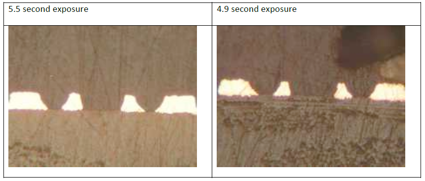
Figure 7 - Etch Factor Comparison for 25µm Space at Different Spray Pressures This also confirms results obtained in earlier testing. Once the spray pressure gets above 20 psi the etch factors remain constant, the only change being etch rate. At this point we have only confirmed that the test results obtained in the early 1990’s when working to reduce undercut in high pin count lead frames. There were many other equipment and chemistry parameters tested than those covered here but those that showed improvement in etch factor (optimum placement of spray nozzles, reduction in topside etchant puddling) were incremental improvements rather than huge revelations and most of those have already been designed into the new generation of equipment beginning in the early 2000’s. Unfortunately, some of the most obvious things that one might think of to improve etch factor (different nozzles, smaller droplet sizes, higher spray pressures) have been confirmed as ineffective. One complicating factor in all these tests was that, no matter what changes we made, the spray was not impinging directly on the copper surface. On the topside there is always an etchant puddle that the spray impacts upon while on the bottom side the spray has to deal with the conveyor rods and wheels which scatters and reduces the velocity of the droplets. The bottom side situation is made even worse by the fact that most HDI is done on thin or flexible substrates, which require more wheels than normal for support. This complicating factor might have disguised any improvements in etch factor that may have occurred in the previous tests. A quick screening test was set up where the conveyor rods containing any wheels that masked the lower spray nozzles were removed giving the nozzles a clear shot at the copper surface without an etchant puddle or masking objects. Tests were run with cone and fan nozzles at several different spray pressures. The results reconfirmed that there is no inherent advantage of one type of nozzle over the other and different pressures changed the etch rate in the fine spaces (as well as that in all the other spaces) but had little, if any, effect on etch factor. Changing the etch speed without changing the etch factor just produces bad test patterns faster. Unfortunately, all the other tests that dealt with equipment modifications to improve etch factor produced the same results, the etch speed could be changed but the etch factor remained the same. Quite frankly, at this point there is very little that can be done to the equipment design that is going to improve undercut without some radical redesign to test some other concepts, but even this is no guarantee of success. So, is there anything else that might be done to improve the situation? An old saw from the days when HDI meant going from 200µm lines and spaces to 100µm lines and spaces says “Under expose and over develop for fine lines”. The question is whether there was and still is any truth to this bit of sage’s wisdom especially considering the considerable improvements in dry film since those years. A screening test was set up to see if this concept was worth following through. 4.1 Dry Film Exposure Tests – The recommended exposure for the dry film used in these tests was step 6 to step 8 on a 21 step density tablet. On the 5000 watt exposure unit used this translated to a 4.9 second exposure time for a step 6 and a 5.5 second exposure time for a step 7. All the previous tests were done using the 5.5 second exposure time. Six test panels were prepared and exposed at times of 5.5, 5.3, 5.1, 4.9, 4.7 and 4.5 seconds respectively. The panels were developed and etched together and the tops and bottoms of the 25µm lines and 75µm lines were measured for comparison. There was not much improvement until the 4.9 second exposure was reached and the resist exposed at 4.7 and 4.5 seconds had adhesion problems. The results for the 5.5 second and 4.9 second exposures are shown below in the table and cross sections.
Figure 8 – Line Width Measurements
Figure 9 – Cross Sections - 5.5 second exposure 4.9 second exposure The results above show that, under the same developing and etching conditions, the 25µm space has etched out more completely for the 4.9 second exposure. More importantly, while the 25µm line is obviously etched more, the dimensions of the 75µm line did not change all that much demonstrating that a lower exposure level may actually help clean out the 25µm spaces faster in relation to the wider spaces. The etch factor for 25µm line did not improve that much but the etching was definitely better. It was hoped that, at the time this paper was solicited, that a full set of tests to confirm these results would be completed by the time the paper was due but other duties have intervened and they have not yet been started. However, the preliminary tests shown here do show that this line of inquiry is worth pursuing. 4.2 Developing Time Tests – Another preliminary test was run with the 4.9 second exposure to compare developing at a conveyor speed set for a 60% breakpoint, as used on the above exposure tests, with a speed set for a 40% breakpoint. Visually, the results seem to show a further slight improvement in the clean out of the 25µm space in relation to the wider spaces. Again, the full set of tests to confirm this conclusion has yet to be completed but the outlook is hopeful. 4.3 Tests for the Near Future – Others have indicated that replacing the free hydrochloric acid by saturating the cupric chloride with sodium chloride, table salt, greatly improves etch factors. This is on the list to be done as soon as possible. Also, there have been developments in spray nozzles and chemical additives for cupric chloride. Samples of both of these will be available by the time this paper is delivered and are also high on the priority list for immediate testing as time allows. The original impetus for this investigation was a request to look into the feasibility of etching 50µm lines and spaces in 35µm foil and 25µm lines and spaces in 18µm foil while using a 30µm dry film. This has to be the ultimate worst case scenario for HDI production but the initial trials clearly defined the problems faced, namely: 1) The etch rates in spaces less than 50µm fall off drastically when compared to wider spaces and 2) because of this, any place where a line of 25µm or less is bounded by a space greater than the line width will be etched out before any spaces the same width as the line can be cleaned out enough to prevent shorts. The ultimate solution to the problems would be to find a way to increase the rate of downwards etch while not increasing the rate of sideways etch. While this goal of increasing the downwards etch without increasing the sideways etch has not yet been attained there were many practical things learned in preparing and etching the test samples that could save a lot of time and effort for anyone engaged in HDI. These observations are listed below although not necessarily in order of importance. The above conclusions are a direct result of the testing done on HDI. The following conclusions are general observations made during the course of sample preparation and testing: |
| Go back to Contents |

| Section 4 |
Thermal Management in High Performance RF and Microwave PCBs John Priday CTO, Teledyne Labtech |
|
John Priday |
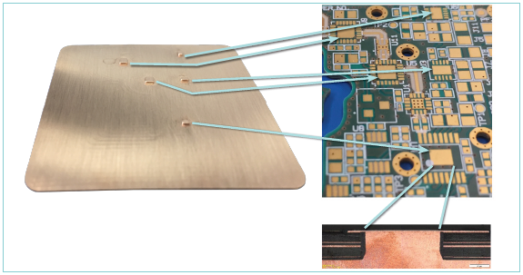
Introduction High density active power devices, such as GaN power transistors, can dissipate significant heat. One of many roles that the PCB has to perform is to channel heat from the underside of the semiconductor device through to the chosen heatsinking scheme as efficiently and effectively as possible. The design challenge is how best to accomplish this while achieving the other trade- offs required such as RF performance, manufacturability and cost. Methods of Thermal Management To improve thermal conductivity one option is to increase the plated wall thickness of the PTHs from the standard 25um, to 100um for example. Often a greater number of smaller PTHs within a ground pad can provide a more effective thermal path than fewer larger PTHs.
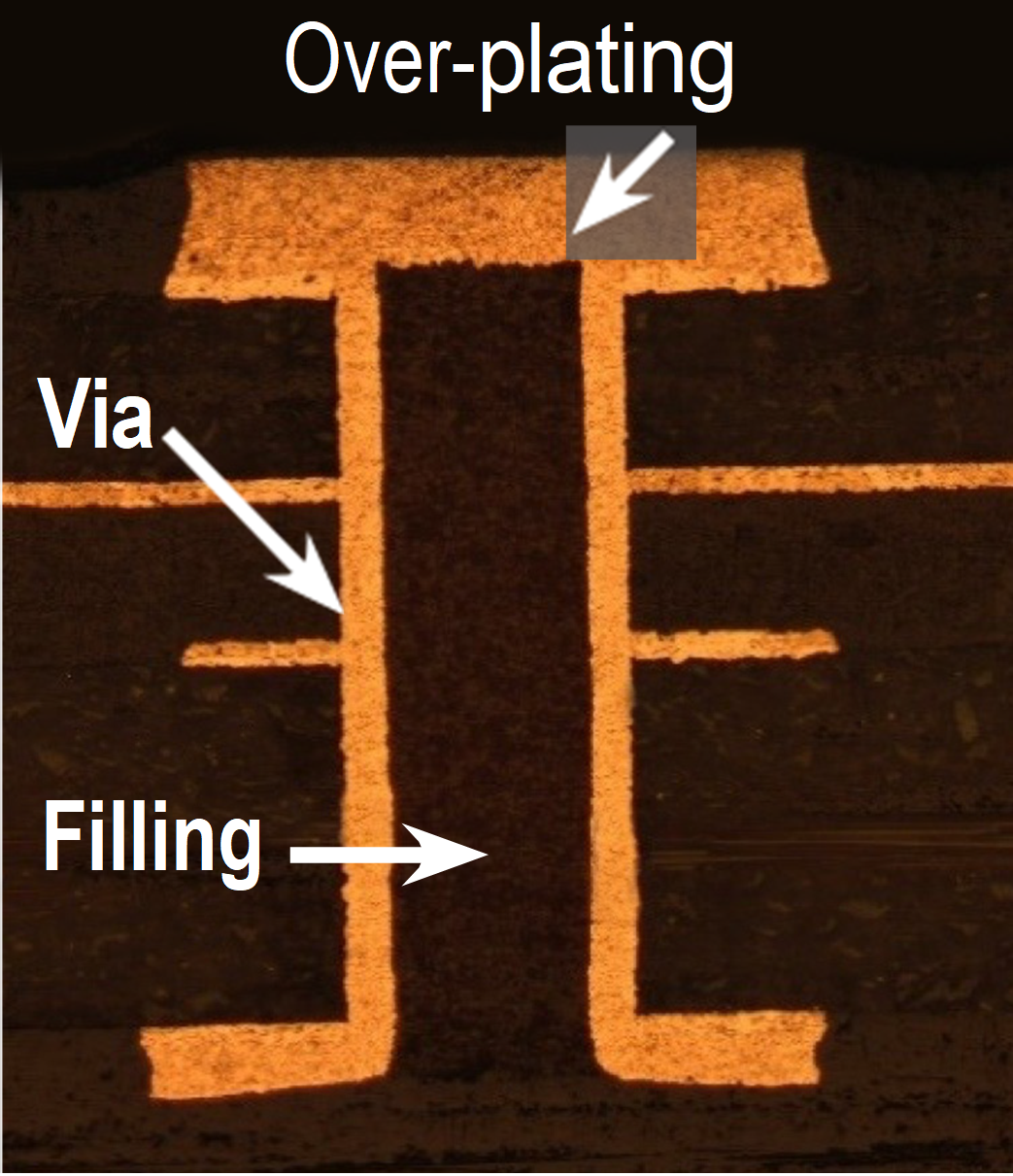
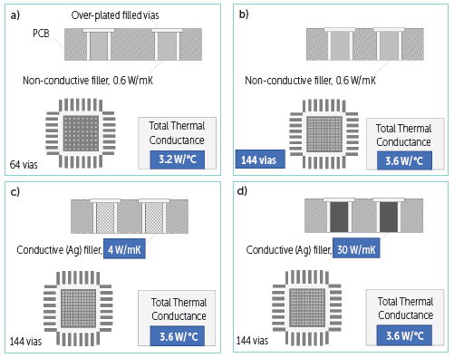
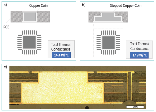
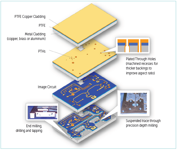
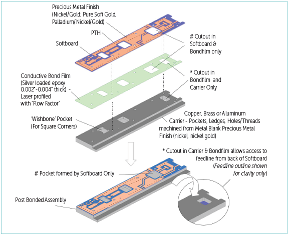
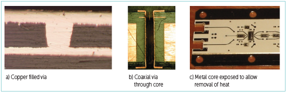
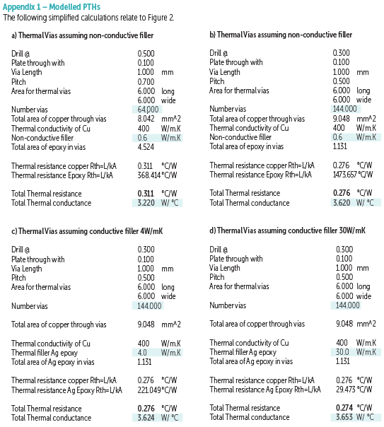
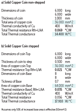
Figure 1: a) Cross-section of filled via Device Ground Pad Figure 1: b) photo of typical device ground pad with over-plated vias just visible Figure 2: Comparison of total thermal conductance of different filled vias There are limits to the effectiveness of heat transfer using a traditional ground pad with PTHs. Figure 2 shows the results of calculations of four different cases, with detailed calculations shown in Appendix 1. Starting with a typical case of PTHs with 0.1mm thickness1 of wall plating, it examines the overall thermal conductance with vias filled with a non-conductive filler (Figure 2 a). Using this as the base case, it then examines increasing the number of vias (Figure 2 b), then changes the filling from non-conductive to conductive silver epoxy of two different thermal conductivities (Figure 2c and 2d). As can be seen the benefit of using Ag epoxy instead of standard non-conductive plug paste to fill the vias is limited and generally not worth the additional expense. 1 While a through-hole wall thickness of 0.025mm is standard in non-thermally challenged applications, we usually recommend 0.1mm where heat transfer is important. Note that if standard 0.025mm plating was used for case 2a, then thermal conductance would only be 0.96 W/°C. Figure 3: Examples of the use of copper coins For many leading edge applications the total thermal conductances shown on previous page are not up to the task. A more effective approach is to use copper coins that are integrated into the circuit’s structure. For ease of comparison, a simple approach is shown in (Figure 3 a), where a 6mm x 6mm square coin is modelled. A more frequently used approach is to have the coin stepped so that heat is not only efficiently conducted away but also spread. This is modelled in (Figure 3 b), and a cross sectional photograph of a real stepped copper coin shown in (Figure 3 c). The larger area of copper provides a larger surface area in contact with the cold wall, providing improved thermal transfer. More detailed calculations are given in Appendix 2. Figure 4: construction of metal-backed circuits Ultimately metal backed circuits offer an ideal solution where large amounts of thermal energy need to be dissipated, as shown in Figure 4. The metal backing can be copper, aluminium or brass as this type of circuit is typically used for solid state power amplifiers (SSPA) and can be of either pre-bonded or post bonded structure. In the case of pre-bonded circuits this is where the substrate is supplied pre-bonded to a thick metal backer. This does limit tracking to a single layer and presents issues during processing as invariably machining operations have to take place after the circuit traces have been formed. Great care needs to be taken to avoid damaging critical circuit features. The advantage is that this provides an excellent ground plane reference. Figure 5: The assembly of post-bonded circuits The post bonded alternative is easier to manufacture in so much as the circuit is produced and verified before being attached to a pre-machined and plated metal backer as shown in Figure 5. Post bonded circuits can have more than a single layer of conductors. Generally, the circuit is bonded to the metal backer using a conductive adhesive layer. For both pre and post bonded circuits the components that require heat to be transferred away are mounted directly onto the metal backer through openings within the circuit. Figure 6: Examples of metal-cored circuits A more complex solution is metal-cored circuits. These can be usefully employed where space is limited and high isolation between RF and control is required in addition to thermal management. Heat being transferred from components to the core can either be through thermal vias or by direct contact through cavities within the circuit that the components are mounted on. Consideration must be given to removing heat from the core. Typically, circuit substrate is machined away from two edges to expose the core so it may be clamped within the chassis to transfer heat. In the case of thermal vias where holes are blind with diameters <0.2mm and depths <0.3mm the holes can be filled with copper using a blind hole plating process. Figure 6 shows examples. Figure 7: Machined copper plane with up-stands, applicable for small circuits Another technique developed by Teledyne Labtech for thermal management on small circuits (<25cm2) and where the overall thickness is limited, yet several devices require thermal management is to employ a machined copper plane with up-stands (pillars). This provides an excellent thermal path way and the heat can be distributed efficiently through the thermal plane for transmission to a cold wall. An example is shown in Figure 7. Summary Appendix 1 – Modelled PTHs Appendix 2 – Thermal Vias assuming non-conductive filler |
| Go back to Contents |

| Section 5 |
Two-Layer Solder Resist Film for High Reliability |
|
Ying Hsuan Chou |
Abstract Key words INTRODUCTION EVALUATION AND RESULTS
Fig. 1. The SEM Image of Crack after TCT Table 1 shows the results of Young's Modulus, CTE and crack occurrence frequency of conventional SR. The Young's Modulus and CTE are measured by tensile tester (Autograph AG-X (Shimadzu Corporation)) and Table 1. The Results of Young's Modulus, CTE and Crack Occurrence Frequency of Conventional SR
Furthermore, in order to understand precisely the correlation between Young's Modulus and crack occurrence frequency, we investigated the crack occurrence frequency of low Young's Modulus SR and compared the results to conventional SR. Fig. 2 exhibits the tendency that as the Young's Modulus becomes higher, the crack occurrence frequency of conventional SR increases significantly. In contrast, SR with 2~3 GPa Young's Modulus is exhibiting below 5% crack occurrence frequency. This result suggests that the material with low Young's Modulus can relieve stress and inhibit cracks from occurring. In our opinion, except for low CTE materials, low Young's Modulus materials also could demonstrate superb crack resistance.
Fig. 2. The Correlation of Young's Modulus and Crack Occurrence Frequency of Conventional SR and Low Young's Modulus SR 2. The New Low Young's Modulus Material It has been reported that, the high loading of inorganic filler in SR has contributed to excellent thermal resistance. Therefore to enhance thermal resistance, we introduced some fillers in the resin matrix and observed the crack occurrence frequency. Table 2 indicates that depending on the contents of filler, the CTE decreases from 70 to 41 ppm, and Young's Modulus increases from 1.3 to 3.0 GPa. In addition, the crack occurrence frequency is almost 0 % when the fillers loading is increased from 0 % to 45 %. In brief, this new low Young's Modulus material could reduce stress efficiently, thus, cracks can be suppressed perfectly. Table 2. The Results of Young's Modulus, CTE and Crack Ratio of Low Young's Modulus Material
As we know, higher filler loading would be a major challenge of high resolution, because the large amounts of filler may cause UV light reflecting and scattering at the interface between the resin and fillers. We observed the resolution of this low Young's Modulus material and summarize in Table 3. It clearly indicates that higher filler ratio leads to higher light scatter during the UV exposure process and thus deteriorates resolution. In conclusion, this low Young's Modulus material possesses excellent crack resistance but shows deficiency in resolution when adding a large amount of filler. Consequently, in order to overcome the challenge of high resolution, we set out to eliminate all fillers. Table 3. The Resolution of Different Filler Content in Low Modulus Material
Then, we confirmed the thermal resistance of this low Young's Modulus material without any inorganic filler by conducting 288ºC 10 sec. × 2 times of soldering float. Fig. 3 apparently exhibits that after solder float test, the solder migrates between SR and copper trace. As explained earlier, low Young's Modulus material would show deficiency in thermal resistance because of weak cross-linked density.
Fig. 3. Surface Observation after Solder Heat Resistance Until now, we have developed a novel low young’s modulus material without any fillers, which achieves perfect crack resistance but insufficient thermal resistance. In order to improve thermal resistance, we stuck a thermal resistance layer which is composed of resins with high thermal resistance and great toughness onto the low Young's Modulus material layer. Namely, we reveal the development of a novel two-layer SR film which consists of low Young's Modulus layer and thermal resistance layer, the configuration of two-layer SR film is shown in Fig. 4.
Fig. 4. The Composition of Two-Layer Solder Resist Film The thermal resistance layer is characterized by toughness, strong heat and chemical resistance, which could withstand rigorous high temperature or chemical process. Also the low Young's Modulus layer could decrease stress effectively and suppress cracks occurring. According to this advanced two-layer structure, we can achieve excellent performances, such as high crack resistance, high resolution, satisfactory thermal resistance, extremely low warpage and high reliability at the same time. Next, we evaluated and explored the characteristics of this novel two-layer SR film, respectively. 3. The Characteristics of Two-Layer Solder Resist Film 3.1 Crack Resistance Table 4. The Results of Young's Modulus, CTE and Crack Ratio of Two-Layer SR Film
3.2 Thermal Resistance
Fig. 5. Surface and Cross Section Observation after Solder Heat Resistance 3.3 High Resolution Table 5. The Resolution of Two-Layer SR Film 3.4 Warpage
Fig. 6. Substrate warpage after cure for conventional SR and Two-Layer SR Film 3.5 Biased - Highly Accelerated Stress Test (B-HAST) Fig. 7. Result of B-HAST for conventional SR and Two- Layer SR Film 3.6 Flip-Chip Assembly
Fig. 8. Process Flow of Flip-Chip Assembly The number of cracks after the thermal shock test is shown in Fig. 10. The crack occurrence frequency of the conventional SR is 65%, whereas that of the new two-layer SR film is as low as 4%. Thus, an overwhelmingly higher crack resistance is attained. Fig. 10. Number of Cracks after TST CONCLUSION In conclusion, the newly developed two-layer SR film with low Young's Modulus is beneficial for the next generation high-density package, especially for the outermost layer of FC-BGA packages and applications that require higher reliability. Moreover, compared to traditional SR, this two-layer SR film show significantly outstanding flexibility, due to the feature of low Young's Modulus. In other words, this two-layer SR film also could have potential application for flexible electronics or rigid flexible electronics.
References |
| Go back to Contents |

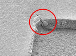
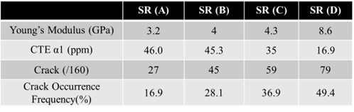
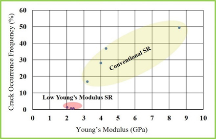
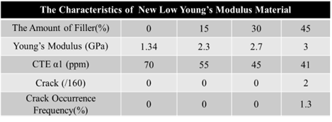
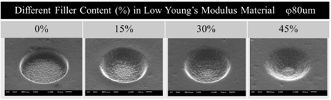
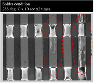
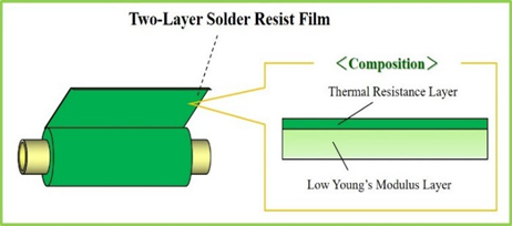
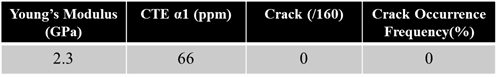
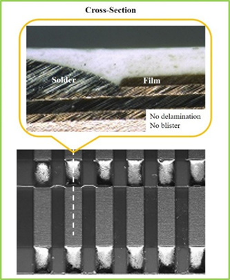
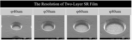
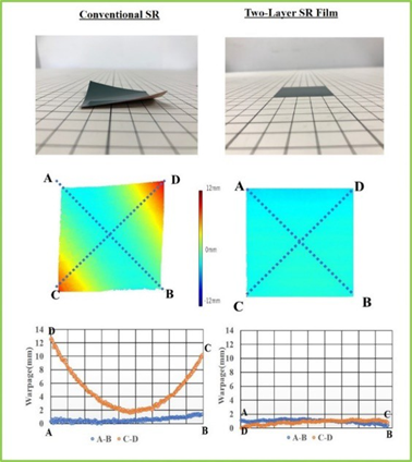
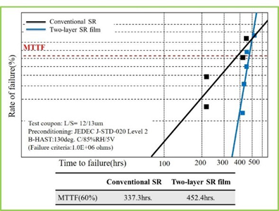
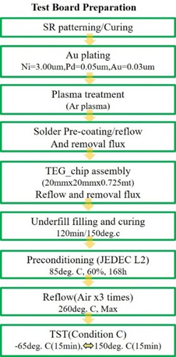
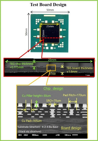 Fig. 9. The Test Board Design
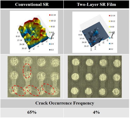
| Section 6 |
Treatment of Polymeric Films Used for Printed Electronic Circuits Using Non-Thermal Plasma |
|
Radu Burlica |
Abstract Introduction The term “plasma” refers to a partially or fully ionized gas composed essentially of free photons, ions and electrons, as well as atoms in their ground or excited states having a neutral charge. These excited and ionized particles carry enough energy to induce chemical reactions at the interface with solid surfaces that change the properties of materials. A DBD reactor has several advantages such as the flexibility of the design and parameters used, the simple setup, low costs and safety in operation. The DBD reactor has proven its ability to modify different substrates such as metal materials, wood or MDF boards, various polymeric materials used in the textile, food or electronics industries. Many studies conducted in recent years have shown that treatment by means of an air DBD reactor at atmospheric pressure improves the properties of hydrophilicity, increases the surface tension of polymers, also changing the roughness of their substrates, and has the advantage of uniform and fast treatment of the entire surface. Polyethylene terephthalate (PET) polyester film has been used in a wide range of applications (packaging, printing, capacitors) because it has some good properties and is easy to recycle. It has a comparatively lower cost which make it very popular despite its inadequate wettability and adhesion properties. Additionally, polycarbonate (PC) has high creep resistance, durability, high hardness and excellent optical transparency, being an attractive polymer. PC is used in a variety of applications such as a substitute for glass. However, the adhesive strength between a deposited film and the PC substrate is weak due to the low surface energy. Therefore, in order to increase the surface tension, these materials can be activated by DBD non-thermal plasma treatment. The main idea of this study is to present the results obtained from DBD treatment of three commercially available polymeric substrate surfaces: Xerox inkjet (polyester), Autostat (polyester) and Lexan (polycarbonate). The materials have been exposed to an air DBD plasma at atmospheric pressure with the aim of modifying the water contact angle (WCA), the adhesion force and the surface morphology. Materials As the non-thermal plasma treatment effect of the considered film surfaces is not constant over time and there are differences depending on the treatment time, it is important to establish how wettability changes with the treatment time, the storage time and the oxidation ageing of these treatments. Industrial plasma treatments involve continuous and rapid treatment surfaces of large quantities of samples. The diminution of treatment time of such individual samples by a few milliseconds can finally result in the reduction in treatment time of thousands of samples by a few minutes. The primary objective of this study is to determine the optimal treatment time of a polymer surface, which is thus very important for industry. Method The polymer layer is placed at a 4 mm distance from E1 electrode. When the voltage applied exceeds the electrical breakdown threshold, an avalanche ionization phenomenon initiates. Due to this phenomenon, a multitude of plasma streamers occur between the electrode and the dielectric glass. The discharge stops when the voltage passes to zero and re-initiates when the voltage changes the polarity. The use of the dielectric barrier prohibits the evolution of the electric discharge into electric arc. At the same time, the charge carriers accumulated at the dielectric surface, quenches the discharge by lowering the field strength. In the discharge, there are many streams exhibiting concurrently and individually, with a lifespan in the range of nanoseconds. Figure 1a: DBD Reactor Schematic Diagram Water Contact Angle Sessile drop method is a common technique used for flat surfaces allowing water contact angles to be measured from the drop profile. In the present paper, the authors used an Ossila Contact Angle Goniometer to assess the WCA and the surface free energy of liquid droplets. A calibrated distilled water drop is settled on the polymer surface using a 25 µL syringe provided with a blunt needle (Φ = 0.47 mm). Figure 2 shows the WCA after 30 s of DBD treatment for the Autostat foil, highlighting hydrophilic enhanced properties.
Figure 2: The WCA for the treated Autostat foil decreased from 71.2◦ down to 19.5◦. There are many factors affecting the WCA including impurities, porosity, surface roughness, or surface free energy. The correlation between the water surface tension and the substrate surface energy is described by Young’s Equation (1) where γsv, γsl, γlv and θ are the interfacial tensions of the solid-liquid, solid–vapor, liquid-vapor interfaces and the Young’s contact angle, respectively:
Results Contact angle measurement is a relevant method to identify the hydrophilicity of polymeric surfaces. The adhesion of a surface is related to its wetting. To assess the surface wetting, contact angle measurement may be performed for a liquid droplet in contact with a solid surface.
Figure 3: The comparison between the immediate effect of plasma treatment on the water contact angle in the case of the tested substrates. There are no important differences concerning the WCA values obtained after the plasma treatment between the different treatment times considered (from 0.2 up to 5 s). The WCA measurements indicate an important increase of contact angle over time, just after DBD treatment. This aspect implies that the treated foil must be used immediately after treatment for the best physical wetting property. After 24 h of storage from plasma application, the WCA values increase up to 45◦ while remaining relatively stable even for more than 70 h of storage. Adhesion force of coatings applied to the materials has also been assessed together with surface profile analysis. This is beyond the scope of this publication and can be referenced below. Conclusions This paper was originally published by MPDI and can be accessed here https://www.mdpi.com/1996-1944/15/5/1919 |
| Go back to Contents |

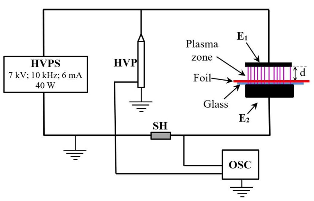
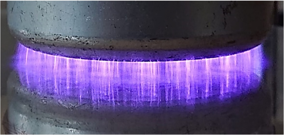 Figure 1b: DBD Discharge Streams
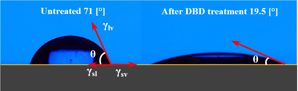
 Equation (1)
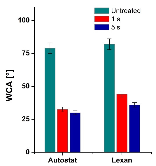
| Section 7 |
Automation & the Journey to your Smart Factory |
|||||||||||||||||||||||||||
|
In Sept and Oct 2022 the ICT held a a series of on-line engineering sessions featuring Happy Holden. They were based on his book "Essential Skills for Engineers" This series of presentations is available now and is free to members and guests. Just register your email below to take you to the link page of the stored webinars. Happy Holden is a retired electronics manufacturing technologist of international repute, He is a contributing Technical Editor to I-Connect007 and Hon Fellow of the ICT There are eight on-line sessions of 60 minutes. The following webinars are available and can be accessed individually or part of a complete training course. Description
Enter your email here to link to the video gallery
|
||||||||||||||||||||||||||||
| Go back to Contents |
| Section 8 | ICT Seminar and AGM 7th March 2023 |
|
|
Widely believed to be the traditional Centre of England, Meriden was a popular venue for a gathering of the UK printed circuit community this month. They braved the forecast of heavy snow for the Institute of Circuit Technology’s annual general meeting to learn about current developments and challenges in a thought-provoking technical seminar and to network with industry peers and contemporaries. Thankfully, the forecasted heavy snowfall did not reach Meriden until after the event; we only had a few flurries, although the weather caused considerable disruption elsewhere in the country. After the formal business of the annual general meeting had been efficiently managed and conducted by ICT Chair Emma Hudson, the early highlight of the evening session was the award of Honorary Fellowship to Rex Rozario OBE. He is credited with being part of the team that developed the first circuit board in England in the 1950s. |
 Alun Morgan Alun Morgan |
The State of Energy The increasing availability of energy has transformed the course of humanity, he said, and the quantity consumed and produced has inevitably continued to increase. Fossil fuels have been supplemented with new energy sources: hydropower, nuclear and more recently with renewable technologies. Although decarbonisation is progressing slowly, it is essential that fossil fuels be displaced in the energy mix at a much faster rate. His charts of global energy consumption and energy production by fuel type illustrated the wide gap that exist between: Groups of principal sources: oil, coal, and gas Morgan then focused on the PCB industry, reviewing world trends and concluding with Europe’s position. Whereas world PCB production has grown from $33.1 billion in 2000 to $60.8 billion in 2019, Europe’s share has reduced from $5.4 billion to $1.9 billion during the same period. But although the number of manufacturers has shrunk from 550 to 173, revenues have remained relatively stable since 2010. The European PCB industry is losing ground due to raw materials and equipment being increasingly difficult to source in Europe, reduced investment capital compared with other regions, and reduced availability of technical resources and workforce. The relative stability of the industry is closely related to its areas of specialisation: strong defence and aeronautics sectors, strong medical sector, and other specialised areas. Presently, the top 30 companies made 70% of the volume in Europe. But the industry was heavily dependent on its supply chain and needed to maintain its critical mass to secure supply continuity. Returning to Morgan’s primary topic, the unique competitive disadvantage Europe suffers relative to its competitors is the cost of energy. In 2021, even before Russia invaded Ukraine, the average price of electricity in U.S. dollars per kilowatt hour was $0.323 in Germany compared with $0.109 in the U.S. and $0.084 in China. In seeking government support, current employment numbers in the PCB industry are not large enough to have meaningful political significance, but defence and security considerations certainly are—a stable European supply base is considered essential—and it is from this perspective that government is being approached. |
|
|
A Focus on Assistive Device Technology A key component of the process is an ink-jettable copper-silver core shell catalyst. This is an alternative to palladium which, although an excellent catalyst, was very expensive and classified as a “critical raw material.” Pure copper nanoparticle colloids are not stable and tend to aggregate over time. Using polyacrylic acid as a shell-ligand produces a stable colloid which enables a uniform electroless copper deposit, but the long-term stability of the ink needs improvement. Adding silver nitrate to a copper nanoparticle/polyacrylic acid dispersion results in an exchange reaction, creating a silver-core shell colloid. This is formulated into an ink-jet printable catalyst, and the silver shell significantly increased the lifetime of the ink. Printed onto a polyester fabric, this ink enables selective metallisation with electroless copper and increasing the number of print cycles increases the copper mass gain. It has been observed that the resistance of the copper deposit decreases with increasing print cycles, there is some difference between warp and weft directions, and resistance increases after each washing cycle. Professor Cobley showed examples of Maturolife prototypes incorporated into assistive footwear, designed to help in the understanding of gait and balance. |
|
|
Things to Consider When It Comes to Thermals He began by reviewing the nature and basic construction of insulated metal substrates and their important datasheet parameters: thermal resistor, thermal impedance, thermal conductivity, glass transition temperature, maximal operating temperature, breakdown voltage and hi-pot withstand. The first and most important datasheet value he considered was thermal resistor or thermal impedance, denoted Rth or Zth, which was measured directly and from which thermal conductivity was calculated. Different test methods gave different values; in the example he used, ISO 22007-2 gave 5W/mK, ASTM E1461 gave 3.3W/mK, ASTM D5470 gave 3.0W/mK, and Bruggeman Modelling gave 12W/mK. Art commented that the ASTM D5470 test was most commonly used; it gave the lowest value because it measured the complete stackup, including the losses in the transfer areas. “Don’t accept thermal conductivity values,” he advised, and demonstrated the sizeable tolerance bands associated with different test methods, implying that a low-cost competitor can quote almost any value and still be in tolerance, depending on the method. Art commented that Ventec is a member of an IPC working group that includes other suppliers and ZFR (Zentrum fuer Waermemanagement) in Stuttgart, to improve the accuracy of the measurement method by tightening thickness tolerances and clearly defining test parameters and probe locations. He asked, “When should you take a deeper look to the datasheet?” and then listed some key points. These include checking which test method has been used for dielectrics with claimed thermal conductivity of 4W/mK and higher, checking in detail how Rth has been measured, and with what tolerance. For values below 0.4, it’s checking the dielectric thickness that has been used as a probe for an ASTM test, questioning why different thermal measurement methods have been used for closely related values quoted on the datasheet in order to improve their appearance, and being suspicious of remarks like “modified” in reference to test methods. Having briefly discussed maximal operating temperature, breakdown voltage and hi-pot withstand, Art mentioned the significance of glass transition temperature in IMS dielectrics compared with rigid laminates, where a lower Tg gave a more resilient product and in combination with a low-expansion aluminium alloy helped to mitigate solder joint cracking. But his over-riding message in specifying an IMS material was, “Be careful, and make sure you understand how it is measured.” |
|
|
Chemical Legislation and Restrictions on Solder Masks The final presentation of the seminar came from Chris Wall, technical director of Electra Polymers, who succeeded in making the subject of chemical legislation and restrictions on solder masks both interesting and enlightening. He explained that the European Union REACH regulation (Registration, Evaluation, Authorisation, and Restriction of Chemicals), which originally came into force in 2007, requires manufacturers and importers of chemicals to register the substances they produce or place on the market in Europe with the European Chemicals Agency (ECHA). The REACH regulation establishes a process for identifying and controlling substances of very high concern (SVHCs). When the UK withdrew from the European Union, the UK government created UK REACH, which adopted all the provisions of REACH (as they were BREXIT at the time) and regulates chemicals placed on the market in the UK. The UK REACH and the EU REACH regulations operate independently of each other and suppliers must ensure that they comply with both regulations where necessary. Clearly, this raises potential issues for global suppliers. Wall pointed out that, currently, the specific relevance to solder mask formulation is to the widely-used photoinitiators “907” (2-methyl-1-(4-methylthiophenyl)-2-morpholinopropan-1-one) and “369” (2-benzyl-2-dimethylamino-4'-morpholinobutyrophenone). Both materials have recently been prioritised for inclusion in the Authorisation List of substances that can only be used under specific conditions, such that the risks are adequately controlled. Certain other components of solder masks are subject to, or likely to become subject to, usage restrictions. The timeline for photoinitiators “907” and “369” is an Authorisation Period of 18, 21, or 24 months from the date of inclusion in the Authorisation List, for manufacturers or importers to apply for authorisation to continue manufacture of import of the material. If this is granted, it will be authorised for use for a further period of time. At the same time, a “Sunset Date” will be notified, which is 18 months after the “Latest Application Date. After the “Sunset Date,” the substance can no longer be used or placed on the market without an authorisation. Wall’s presentation raised many questions from the audience, to which he responded reassuringly, stressing that there is no immediate need to panic, and that Electra and its counterparts in the industry have been working hard to develop liquid photoimageable solder mask formulations of equivalent performance which do not contain the “907” or “369” ingredients. |
 Bill Wilkie Bill Wilkie |
Bill Wilkie brought the formal proceedings to a close, with warm thanks to all who braved the weather forecast to participate, and wished everyone a safe journey home through the snow. Note: Much thanks to Alun Morgan for the beautiful images. |
| Go back to Contents |
 Rex Rozario
 Andy Cobley
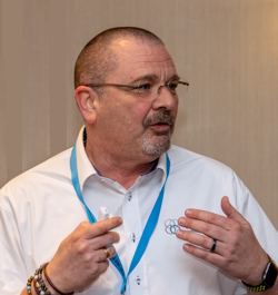 Robert Art
 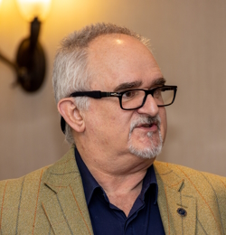 Chris Wall
|
Members News |
|
|
Honorary Fellows The following members have been awarded Honorary Fellowship grading in recognition of their contribution to our industry and the ICT. They all have an outstanding reputation and it is fitting that the The Institute is able to show gratitude to them by awarding them this status. David Burling Bill Wilkie – Membership Secretary – March 2023 |
|
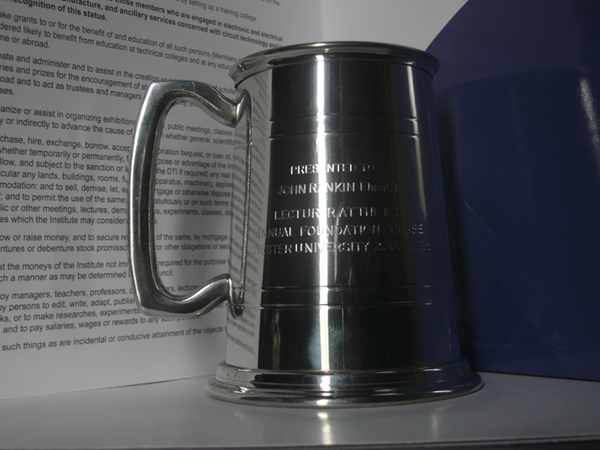
 John Rankin John RankinFInstCT |
This year we say thankyou to John Rankin, who began PCB life at Bepi and was training manager before joining Morton. John has given the photomechanical processes lecture since 2005 and is now retiring. John has been presented with an inscribed Pewter Tankard in recognition of his help and dedication to the Foundation Course.
Presented to |
|
|
|
Industry News |
|
| A-Gas Electronic Materials |
A-Gas EM Gold Investors in People Award |
| Electra Polymers | The Impact of REACH Pete Starkey and Ashley Steers of Electra Polymers Ltd discuss SVHC, REACH and changes to solder mask processes and products. Read more... |
| GSPK Circuits | Power Electronics Busbars GSPK is the leading manufacturer for Heavy Copper PCBs for Power Electronics. It is not uncommon for a customer to ask us to manufacture a 70oz PCB with inner layers to 15oz. We can embed copper so that even with mix copper weights the outer layer will have a smooth planar finish. Read more... |
| Merlin Circuit Technology | Merlin Circuit Technology Ltd – NADCAP RE-Approval Merlin Circuit Technology Limited are very happy to announce that we have been re-approved for the NADCAP Accreditation. This is excellent news for Merlin and highlights the dedication of our staff at all levels within the company – working as a team to again achieve this Internationally recognised accreditation. Read more... |
| Newbury Electronics | Sponsors of Southampton University Formula Student Team We are very pleased to announce that Newbury Electronics Ltd are sponsors of Southampton University Formula Student Team for 2023. Thanks to our fast turnaround manufacture of their PCB designs they have been able to accelerate their electronics development and start manufacturing their 2023 vehicle. Read more... |
| Taiyo |
New Partnership for Taiyo Circuit Automation and Viking Test Ltd. |
| Trackwise Designs | Length-unlimited Flexible Circuits Inspire Diverse New Applications Trackwise Designs plc has revealed that its length-unlimited flexible printed circuits (FPCs) are driving product innovation in many sectors including agritech, wearables, industrial sensing and heating elements. As design engineers apply the Trackwise-patented Improved Harness Technology™ to solve their design challenges and enable smarter and more advanced products. Read more... |
| Ventec International | High Thermal Conductive Metal Base Laminate Ventec are pleased to announce the launch of its latest high thermal conductive metal base laminate VT-4BC designed for use in applications requiring excellent performance in thermal management including super bright lighting, power modules, controllers, motor drives and rectifiers. Read more... |
| Go back to Contents |
Membership News |
||||
|
|
New Corporate Members New Members |
|||
| Go back to Contents | ||||
| Section 12 | Corporate Members of the ICT | |
| Adeon Technologies BV | www.adeon.nl | |
| A-Gas Electronic Materials | www.agasem.com | |
| Amphenol Invotec Ltd | amphenol-invotec.com | |
| Atotech UK Ltd. | www.atotech.com | |
| CCE Europe | www.ccee.co.uk | |
| CCI Eurolam | www.ccieurolam.com | |
| Electra Polymers Ltd | www.electrapolymers.com | |
| The Eurotech Group | www.eurotech-group.co.uk | |
| Exception PCB Solutions | www.exceptionpcb.com | |
| Faraday Printed Circuits Ltd | www.faraday-circuits.co.uk |
|
| Graphic plc | www.graphic.plc.uk | |
| GSPK (TCL Group) | www.gspkcircuits.ltd.uk | |
| Macdermid Alpha | www.macdermidalpha.com | |
| HMGCC | www.hmgcc.gov.uk | |
| Holders Technology UK | ww2.holderstechnology.com | |
| Jiva Materials | www.jivamaterials.com | |
| Merlin Circuit Technology Ltd | www.merlinpcbgroup.com | |
| Merlin Flex Ltd | www.merlinpcbgroup.com | |
| Minnitron Ltd | www.minnitron.co.uk | |
| Newbury Electronics Ltd | www.newburyelectronics.co.uk | |
| Photomechanical Services | www.creekviewelectronics.co.uk | |
| Pillarhouse International | www.pillarhouse.co.uk | |
| PMD | www.pmdchemicals | |
| Polar Instruments | www.polarinstruments.com | |
| Schmoll Maschinen | www.schmoll-maschinen.de | |
| Stevenage Circuits Ltd | www.stevenagecircuits.co.uk | |
| Strip Tinning Ltd | www.striptinning.com | |
| Taiyo America, Inc | www.taiyo.com | |
| Trackwise Designs Ltd | www.trackwise.co.uk | |
| Ventec Europe | www.ventec-europe.com | |
| Zot Engineering Ltd | www.zot.co.uk | |
| Go back to Contents |
ICT Council Members |
|
|
Council Members |
Emma Hudson (Chair), Andy Cobley (Past Chairman), Steve Payne (Hon Deputy Chairman), Chris Wall (Treasurer), William Wilkie (Technical Director, Hon Sec, Membership & Events), Richard Wood-Roe (Journal Editor & Web Site), Jim Francey, Martin Goosey, Lynn Houghton, Pete Starkey, Francesca Stern and Bob Willis, |
Editors NotesThe ICT Journal |
|
|
Richard Wood-Roe |
Instructions / Hints for Contributors 1. As it is a digital format the length is not an issue. Short is better than none at all! 2. Article can be a paper or a text version of a seminar or company presentation. Please include data tables, graphs, or powerpoint slides. We can shrink them down to about quarter of a page. Obviously not just bullet points to speak from. 3. Photo's are welcome. 4. We would not need source cross references 5. Title of presentation - Of course! Date, Job title of Author and Company represented. 6. An introductory summary of about 150 words would give the reader a flavour of what it's all about. 7. Style - we don't want out and out advertising but we do recognise that the author has a specialism in the product or process that will include some trade promotion. Sometimes it will be a unique process or equipment so trade specific must be allowed. 8. Date and any info relating to where or if this article may have been published before. 9. We can accept virtually any format. Word, Powerpoint, publisher, PDF or Open Office equivalents. 10. Also, to make it easy, the author can provide a word file to go along with his original powerpoint presentation and I/we can merge it together and select the required images. 11. A photo of author or collaborators. I really do look forward to receiving articles for publication. Richard Wood-Roe |