
The Journal of the Institute of Circuit Technology Vol 11 No 3 November 2018 |
|
| Links to Contents | Section |
| Calendar of Events | 1 |
| 2 | |
| Council Members | 3 |
|
Alun Morgan, Martin Cotton, Peter Coakley, Rex Rozario, Anthony Lloyd, New Members Update. |
4 |
|
ICT Annual Symposium at The National Motor Museum, 5th June 2018 |
5 |
| 6 | |
|
Boron Arsenide – a novel high thermal conductivity material for electronics applications. |
7 |
|
Increasing the Performance of Organic PCBs at Higher Temperatures |
8 |
| 9 | |
| 10 | |
| Corporate Members | 11 |
| Publishers Notes | 12 |
| Section 4 |
Membership News |
 |
Alun Morgan, Chairman of the EIPC, has been named Technology Ambassador for Ventec International Group. In support of a common mission to promote the next generation's progress in PCB material design, Alun will apply his extensive background and expertise in advocating for the Taiwan stock exchange listed company as an advisor and ambassador. Read more... |
 |
Please join us in wishing Martin Cotton, Director OEM Projects, a very happy retirement. Martin Cotton’s career spans over 51 years with 45 spent in the Printed Circuit Board Industry. After much consideration and careful planning, Martin announced his retirement at the end of September 2018 and will be gradually working his way out of the company by the end of the year.Martin will be retiring from full-time employment to concentrate on commercializing his many patents.Read more... |
 |
Ventec International Group Co., Ltd. has appointed Peter Coakley as sales director UK. Effective July 1, Peter takes over the responsibility for the strategic leadership of UK sales activities that will contribute to the overall growth strategy of the company. Read more... |
|
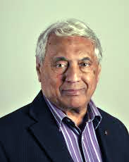
Rex Rozario |
Rex and Ruth were married at Lympstone Manor. Saturday 7th July 2018 |
 |
GSPK YORK CITY LEGEND – SUPPORTING LOCAL CHARITY GSPK and it’s employees have a policy of supporting Local and National charities each year and Anthony was glad to put his super skills to work. The event has received positive feedback from many of the 596 York City supporters who attended the Fundraising match. Proceeds will be split between the Supporters’ Trust and The Offside Trust – an organisation that aims to combat child abuse in sport. Read more... |
| Bill Wilkie: Technical Director and Membership Secretary |
NEW MEMBERS ASSOCIATE MEMBER MEMBER Jonathan Conboy Sun Chemical Ltd FELLOW Martin Wickham National Physical Laboratory |
| Go back to Contents |

| Section 6 |
ICT Hayling Island Seminar September 2018 |
|
Bill Wilkie Technical Director ICT |
After an extreme summer heat wave had left trees dehydrated and struggling to morph into their customary display of reds and golds, the leaves were brown and brittle as the great and good of the UK printed circuit board industry crossed the bridge from the mainland of the south coast of England to Hayling Island for the autumn seminar of the Institute of Circuit Technology on September 20, 2018. ICT technical director Bill Wilkie welcomed delegates to what has of recent years become a highlight of the Institute’s seminar programme and remains an extremely popular event. He emphasised the role of ICT in keeping its membership aware of market trends and emerging technologies, with reference to the demise of some big-name companies who had either failed to recognise those trends or ignored those technologies that had initially appeared to be well-out-of-the-box but had subsequently become mainstream. He introduced a seminar programme that included a discussion of developments in semi-additive flexible circuit fabrication, an update on global and European market statistics and forecasts, a review of the state-of-the-art in dry film photoresist characteristics and capabilities, and an example of how a good presenter can make potentially dreary legal stuff remarkably interesting. |
|
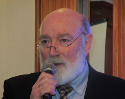
Steve Payne, Cirflex Technology and ICT Vice Chairman |
First speaker was ICT vice-chairman Steve Payne, from management and technical consultancy Cirflex Technology, with a presentation entitled “SAP—a Case Study for Flex.” Payne explained that although the principles of semi-additive processing (SAP) had been established for many years, modified semi-additive processes had become popular in IC substrate production, and were poised for widespread adoption as enabling technologies in the manufacture of ultra-fine-line PCBs, particularly in applications such as the latest smartphones. The basis of the SAP concept was to use pattern plating to selectively build up the thickness of copper tracks on a very thin base copper, in order to reduce undercut effects when the base copper was etched away. Clearly, the thinner the base copper, the less the undercut, and hence the better the capability to fabricate very fine tracks and gaps. Payne referred to a case study where semi-additive processing had been employed in the fabrication of flexible circuits with tracks and gaps of 25 microns and less. Obviously, it had been necessary to start with extremely thin base copper, and the choices were to procure flexible materials manufactured with very thin copper foil, to reduce the thickness of standard copper-clad flexible material by controlled etching, or to seek an alternative technique such as sputter-deposition of copper. In Payne’s example, reel-to-reel DC magnetron sputtering had been used to deposit very thin copper onto polyimide film. Because this deposit thickness could be less than one micron, special techniques were demanded in photoimaging and pattern plating processes, but etch undercut was practically eliminated and track and gaps of 25 micron or less could be achieved in good yield. The sputter process could also metallise laser-drilled through-via holes. Payne discussed the principles of DC magnetron sputtering, described a typical process flow for semi-additive 2-layer flex, and showed examples of flexible circuitry produced using this technology, which was in production in certain locations in the U.S. and the Far East. |
|
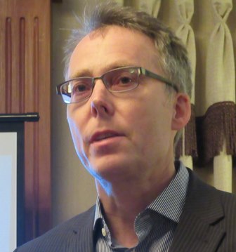
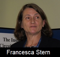
Francesca Stern Market Analyst and ICT Council Member |
Market analyst and ICT council member Francesca Stern delivered her eagerly-awaited annual review of the global outlook for the PCB and electronics industries. She began with a well-illustrated and authoritative overview of trends in electronics and PCB production in Europe, USA, Japan and China, commenting that there appeared to be a slight slow-down in 2018 as compared with 2017. Consumer electronics production in Germany was definitely moving downwards. It was encouraging that figures for the UK electronics industry were currently looking better than for some other major Western European producers, but growth forecasts for the next two years indicated that the UK would show a downturn later in 2018. The U.S. was currently performing quite well, especially in instrumentation and military areas, but was also expected to show a downturn later in 2018. Japan continued to show negative growth. In China, base stations for 5G were a significant growth area, but so far 2018 had not been a good year for China overall. Global PCB production was valued at around $63 billion in 2017, of which the UK’s share was £128 million with a slight increase to £130 million predicted for 2018. |
|
John Cornforth Account Manager Macdermidenthone Electronic Solutions |
“Imagine Imaging” was the headline of the third presentation, given by MacDermid Enthone’s John Cornforth, a regular contributor to the ICT foundation course. He described how a relationship had been established between MacDermid Enthone and Hitachi Chemical for the supply of dry film photoresist to the European PCB and metal finishing industries, and discussed the logistics of the supply chain. The products were manufactured in Malaysia and shipped as master rolls to a new cleanroom facility in the UK for slitting to the widths and lengths required by the European market, for which all of the necessary certifications were in place. Cornforth discussed electronics industry trends and the imaging demands of current and emerging PCB manufacturing technologies, an example being semi-additive processing for which thinner resists were required. With reference to Hitachi’s product portfolio, which also included materials for the microelectronics industry, he outlined typical applications for a range of different product types, and reviewed typical customer future requirements which included faster exposure, finer lines, improved adhesion, better tenting and faster stripping. There was a trend for LDI exposure systems to employ shorter wavelengths, and Cornforth described the characteristics of a new dry film specifically developed for 405 nm exposure. |
|
Colin Martin of ParaChem Consulting Chemists |
The final presentation, given by Colin Martin of ParaChem Consulting Chemists, was an update on the REACH regulations. He remarked that of the four presentations of the evening his might well be the stinker, especially as it was on the subject of environmental compliance and the range of “interesting work” that this invariably created. REACH, a European Union regulation concerning the Registration, Evaluation, Authorisation & restriction of CHemicals, applied to most businesses in the UK in some way, and was a significant consideration in the PCB industry where it impacted the use of chemicals “from cradle to grave,” both upstream and downstream. Martin gave an introduction to the REACH regulations, and commented that although this was European legislation, the requirements applied to any product sold into the European Union and would continue to apply in the UK after “Brexit.” He discussed the significance of REACH in the PCB industry and explained the meaning of “substances” in “articles,” and the declarations PCB producers were obliged to make to their customers if “Substances of Very High Concern” (SVHCs) were present at more than 0.1% w/w in an “article,” including providing “sufficient information, available to the supplier, to allow safe use of the article including, as a minimum, the name of that substance.” Guidance was available in Article 33 of the REACH regulations. Specific examples of SVHCs included boric acid, potassium chromate and various organic materials. As of June 2018, further substances had been added including lead, which was still used in some electronics soldering applications. This meant that boards assembled using lead-based solders would need to be weighed to determine if the lead was present at more than 0.1% w/w. Martin commented that HASL-finished boards could well contain more than 0.1% w/w of lead. Compliance statements were necessary for every single product made, so it was important to implement an efficient and systematic approach. ParaChem had developed an online database called ReachWARE, which could assess products and produce compliance reports. Compliance had been a legal requirement since 2009 and failure to make a declaration was a criminal offence, although Martin believed that no-one had so far been prosecuted and, although there was no choice but to comply, there was no need to despair! |
|
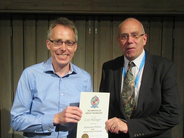
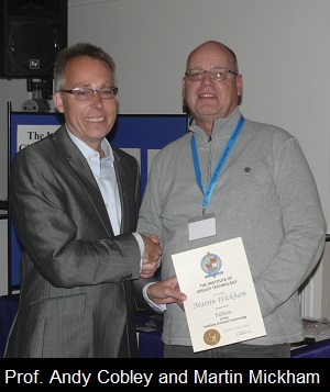
Martin Wickham, well known for his work at the National Physical Laboratory, had recently been elected a Fellow of the Institute and he was presented with his fellowship certificate by ICT chairman Professor Andy Cobley, who then thanked the speakers for sharing their knowledge, and MacDermid Enthone for supporting the event. And special thanks to Bill Wilkie for his diligent organising work behind the scenes, and for chairing the seminar. I am grateful to Professor Martin Goosey for his assistance in preparing this review. |
|
| Go back to Contents |
| Section 7 |
Boron Arsenide Boron Arsenide – a novel high thermal conductivity material for electronics applications. Professor Martin Goosey |
||||||||||||||||
|
Visiting Professor in Sustainable Electronics Manufacturing - Loughborough University |
Since the birth of the modern semiconductor industry, thermal management has often been an important issue for many electronic components, devices and systems. However, the removal of heat and the control of operating temperatures has taken on an increasing significance as the levels of integration and miniaturisation have continued to drive more and more functionality into ever smaller volumes. There are also many new and emerging applications, such as in LED lighting and electric vehicle power management systems, where the removal of heat is a key requirement in terms of performance and reliability. Whether it is at the semiconductor, PCB, or system level the need for new materials and design solutions that can improve thermal management has never been greater. Over the last fifty years or more the industry has gradually developed a range of materials, assembly methods and packaging approaches that are specifically designed to address the need to remove heat. Typical early examples included the use of suitable large metal heatsinks and high thermal conductivity materials such as beryllia. More recently, the benefits of other materials such as aluminium nitride substrates and metal cored PCBs have been exploited and, for the future, the new wonder material graphene seems to have the potential to make a significant contribution. From the PCB perspective, numerous approaches have been developed that are often application specific, but they all rely on removing heat from the source in order to reduce operating temperatures and improve reliability. One material that has recently come to attention for its high thermal conductivity is boron arsenide. Boron arsenide, as its name confirms, is a chemical compound comprising equal quantities of boron and arsenic and it thus has the chemical formula BAs. Boron is from group three of the periodic table, while arsenic is from group five, so BAs is a three-five (III-V) compound and it is a semiconductor in a similar manner to gallium arsenide, which has long been used in a range electronics applications. BAs has a cubic crystal structure (sphalerite) and a very high melting point (2076 °C). It has been used in the past to form ternary and quaternary semiconductors by alloying it with gallium arsenide and there have also been suggestions that it might find use in photovoltaic applications, although this doesn’t seem to be the case so far. To date, it has been reported as being difficult to produce, with samples showing a significant level of disorder and defects in their crystal structures. This had prevented some of its more interesting material properties, such as high thermal conductivity, from being realised. Theoretical modelling (1) by a team at the US Naval Research Laboratories in Washington, USA, had suggested that BAs should have a very high thermal conductivity, somewhere over 1,300 W/mK, which is much higher than most of the other well-known high thermal conductivity materials and closer to diamond. However, because of the high level of defects found in most samples produced until recently, the maximum thermal conductivity achieved was below 200 W/mK. While this figure is still good, it was nowhere near what was thought to be possible. That all changed in July this year, when researchers in the School of Engineering and Applied Science at the University of California, Los Angeles, USA, published the results of their work to synthesise BAs crystals with no defects. In a paper entitled ‘Experimental observation of high thermal conductivity in boron arsenide’ (2), Yongjie Hu et al reported that they had synthesized BAs single crystals with undetectable levels of defects. These single crystals were found to exhibit thermal conductivities of around 1,000 W/mK at room temperature. This thermal conductivity is compared with the values for some other popular high thermal conductivity materials in Table 1 below.
Table 1: Example thermal conductivities of various materials As can be seen, the thermal conductivity of BAs, while being high, is significantly below that of graphene, which has the potential to provide thermal conductivities of up to 5,000 W/mK. However, graphene is effectively a two-dimensional material that exhibits a high level of anisotropy in its thermal conductivity. While graphene might offer significant advantages, its utility is often limited by the various interfaces, contacts, and surrounding materials with which it is in contact in many practical applications. However, in the case of BAs, there are likely to be many specific areas and applications in which it will be eminently suitable. The high thermal conductivity BAs reported in the Science paper was produced using a modified chemical vapour deposition (CVD) process, which would seem to suggest that the likely applications would, at least initially, be in the fabrication of semiconductor devices, where such techniques and the related equipment are commonly employed. Martin Goosey References |
||||||||||||||||
| Go back to Contents |
| Section 8 |
Increasing the Performance of Organic PCBs at Higher Temperatures Martin Wickham, Vimal Gopee, Adam Lewis and Christine Thorogood National Physical Laboratory, Teddington, UK |
|
Martin Wickham Senior Research Scientist at National Physical Laboratory (NPL) |
This paper was presented at the SMTA Europe, Electronics in Harsh Environments Conference on 24-26 April 2018 in Amsterdam, Netherlands. The conference focused on building reliable electronics used in power electronics and harsh environments. Introduction Aerospace, engine management systems, oil and gas resources, automotive and power management for hybrid/electric vehicles are some applications where elevated temperatures, pressures and aggressive media are involved. As a result of emission legislation (e.g. CO2 emissions) and the drive for improvements in efficiency, the market for these applications is growing rapidly. As electronics move ever closer to the source of combustion (engines) or drill heads (down hole applications), normal lead-free solders (melting at ~220 oC) and organic FR4 PCBs (<140 oC) become unsuitable due to the ambient temperatures exceeding operating limits. Traditionally these high-reliability applications have had to use high cost alumina technologies. Alumina substrates are hard to machine and use gold, silver or palladium conductor inks interleaved with dielectric material requiring successive firing at high temperatures (600 oC). The result is very reliable and stable but very high cost in terms of monetarily outlay (tooling £15k) and energy use. Through-hole component assembly and through-substrate vias are also difficult to produce with ceramic technology. Using polymeric based systems at temperatures above 175 oC can be problematic. Whilst several substrates with decomposition temperatures (the temperature at which a 5% weight loss occurs by thermal gravimetric analysis (TGA) (Reference 3)) above 400 °C and/or T288 (measures time to delamination at 288 °C (Reference 4)) times of greater than 60 mins (References 1, 2), these figures make no account for the performance of the copper (Cu) cladding. Previous work by the authors to develop a high temperature solder alternative (Reference 5) showed that the weak link in the system was the electroless nickel/immersion gold (ENIG) finished Cu tracking connecting the components.
Figure 1 Figure 1 shows track failures generated after 6500 hours aging at 250 oC. Here the Cu track has oxidised causing embrittlement and subsequent fracture resulting in electrical failures.
Figure 2 Figure 2 shows x-ray dispersive spectroscopy (EDAX) scans of cross-sections of similar samples before and after 3000 hours at 250 °C. Increased oxygen content can be seen in the aged sample.
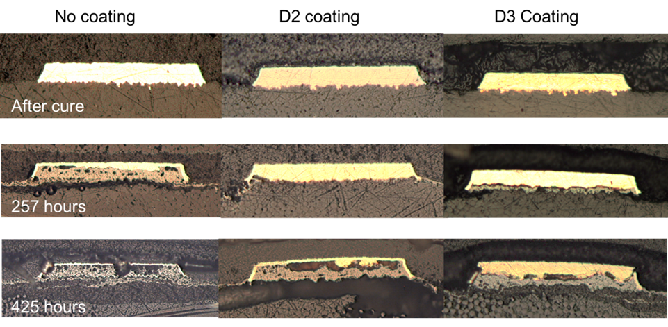
Figure 3 The Cu failures occurred earlier and with higher frequency in samples soldered using high melting point solder. This is shown in Figure 3 where the failure rates of high temperature conductive adhesives (designated D2 and D5) manufactured by curing the adhesives at 250 °C are compared with the soldered samples (HMP) manufactured above the melting point of the solder (~300 °C). Full pad refers to solder paste or adhesive printed over the full area of a normal 1206 component pad or land. For half pad samples the adhesive was only printed on the inner half of the pad or land (i.e. underneath the component). The increased temperatures of HMP reflow have caused the extra degradation of PCB and subsequent higher failure rate of the samples (Reference 5). The premature failures of the Cu tracking on the test vehicles led the authors to consider using high temperature organic coatings to inhibit oxide formation. Phase 1: Initial Trials of Coatings Trials of specially formulated coatings were conducted on glass-reinforced polyimide substrate samples with surface tracks with an ENIG finish on Cu. The samples were dip coated with two coatings (designated D2 and D3) and cured at 250 °C for 30 mins. Control samples were left uncoated. The samples were then aged for up to 425 hours at 250 °C. Examples were micro-sectioned at 0, 257 and 425 hours of aging.
Figure 4 Optical images can be seen in Figure 4. The development of the Cu can clearly be seen as the darker area on the underside (lower) of the track. The outer (upper) surface of the Cu was protected from oxygen ingress by the ENIG surface finish. Thus the rate of oxide formation is controlled by the rate that oxygen can permeate through the underlying substrate. The coated samples showed reduced oxidation compared to the unprotected samples with the slowest rate being exhibited by the D3 samples. This material was therefore chosen for further evaluation for the remainder of the project.
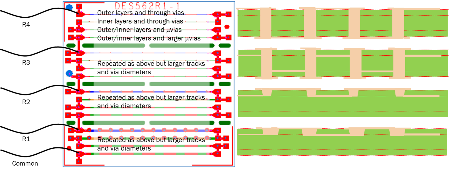
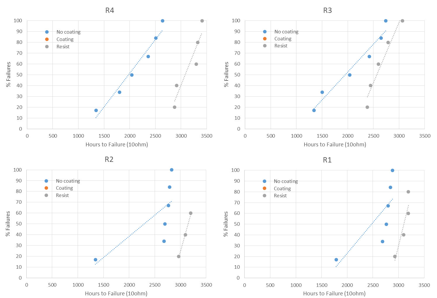
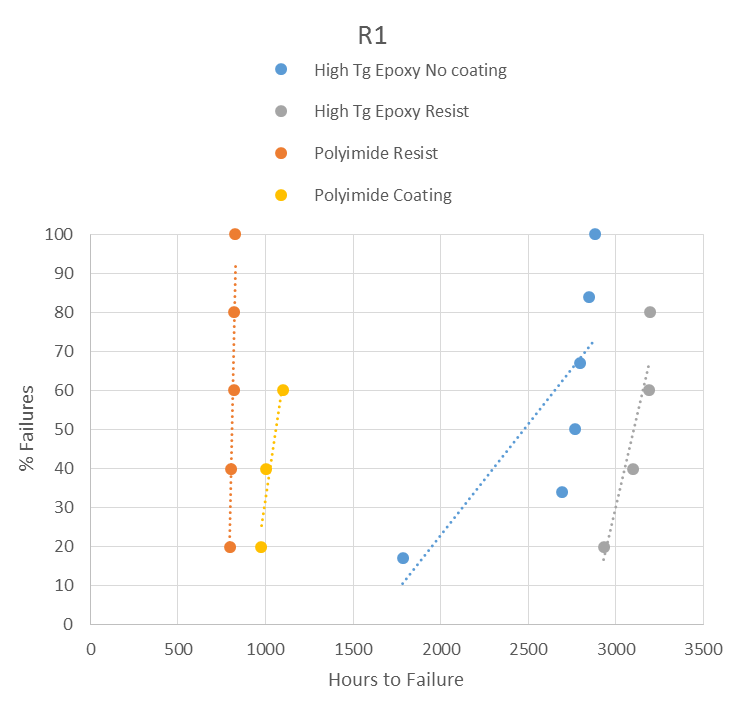
Figure 5 Phase 2: Performance assessment of coated multilayer test vehicles To determine the performance benefits of the high temperature coating, a four layer PCB test vehicle was designed.A schematic of the PCB and main features of the design can be seen in Figure 5. The design consisted of 4 measurement circuits (designated R1 to R4) of decreasing feature size. The main features of each circuit were as follows: R1: Vias = 5X mm Ø, Tracks = 8Y mm R2: Vias = 2.5X mm Ø, Tracks = 4Y mm R3: Vias = 1.5X mm Ø, Tracks = 2Y mm R4: Vias = X mm Ø. Tracks = Y mm Each measurement circuit consisted of four daisy chains connected in series. These circuits consisted of: Upper chain: Outer layers and through vias Upper middle chain: Inner layers and through vias Lower middle chain: Outer/inner layers and mvias Lower chain: Outer/inner layers and larger mvias Test vehicles were fabricated in a glass-reinforced polyimide laminate system (designated PI) and a high Tg (~260 °C) glass-reinforced epoxy system (designated EP). Thermally resistant wires were soldered to the PCBs using a high Pb content solder to allow continuous monitoring. Control samples were left uncoated. To coat the coated samples, they were dip coated with the D3 coating and cured at 250 °C for 30 mins. This method ensured complete coating of the entire PCB. A resist version of the coating was developed which was screen-printed onto the upper (Resist) and upper and lower surfaces (Resist1) of the PCB with annular ring clearances around vias and uncoated edges. The test vehicles were subjected to isothermal ageing at 250 °C for up to 3500 hours. The electrical resistance of each of the four measurement chains was logged every minute using a switching system and digital resistance meter using 2-probe resistance measurements.
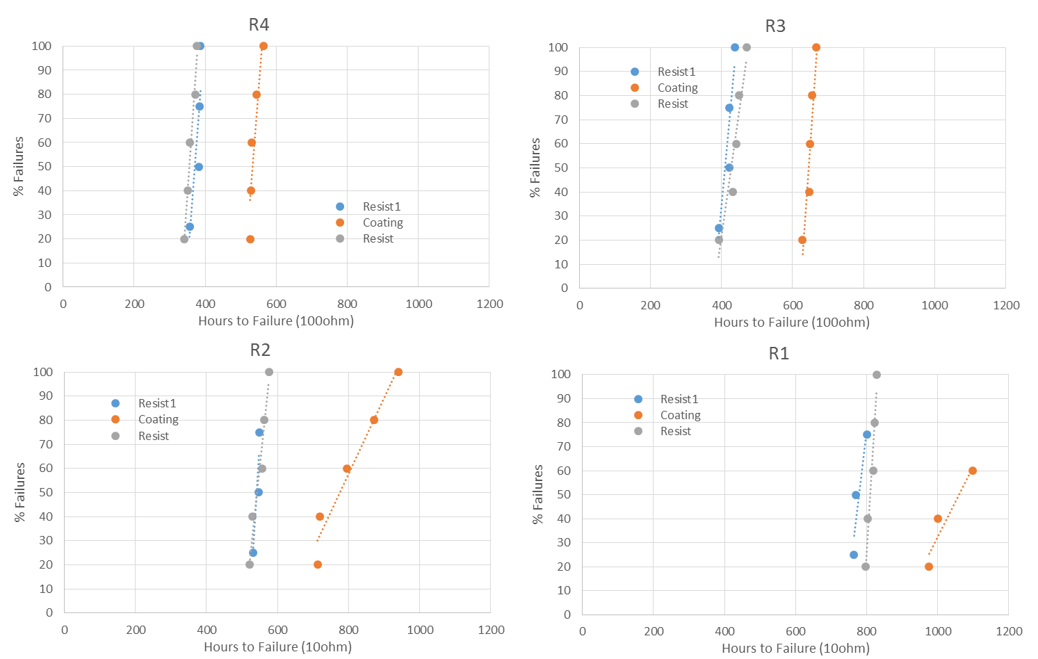
Figure 6 Results Figure 6 shows the failures for each measurement chain as a function of time for the polyimide samples. The failure criteria was a chain resistance of greater than 10 ohms. As the feature size increases (R4 < R3 < R2 < R1), it can be seen that the hours to failure increase corresponding, due to the increased volume of Cu requiring oxidation before failure occurred.
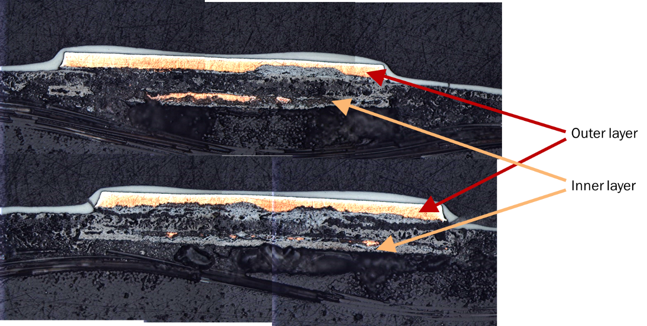
Figure 7 Figure 7 shows some typical micro-sections of the polyimide substrates after ageing. The thinner inner layer can be seen to be almost totally consumed by oxide, with the upper surface of the outer layer again protected by the PCB surface finish. The coated samples (in orange) performed better than both the resist and uncoated samples, extending the typical time to failure by greater than 50% compared to the resist coated examples, indicating that complete encapsulation of the test vehicle was required to achieve the best performance.
Figure 8 For the high Tg epoxy substrates the resist was only applied to one surface of the substrate. Figure 8 shows the failures for each measurement chain as a function of time for the high Tg epoxy samples. The failure criteria was again a chain resistance of greater than 10 ohms. After 3500 hours of testing at 250 °C, the coated examples exhibited no failures, indicating an improvement in performance of at least 100% compared to uncoated substrates. As the feature size increased (R4 < R3 < R2 <R1), it can be seen that the hours to failure increase corresponding for the uncoated substrates, due to the increased volume of Cu requiring oxidation before failure occurred. The failures in the resist coated samples is largely independent of feature size. Figure 9 Figure 9 shows a comparison of failures rates for high Tg epoxy and polyimide substrates for the R1 features size. This indicates that the high Tg epoxy system substrates showed improved performance compared to the polyimide substrates. Conclusions This evaluation of substrate materials has shown that by careful choice of material and the use of innovative coating materials, the ability to survive isothermal ageing at 250 °C can be significantly improved. The polyimide system evaluated here showed significant resistance increases after approximately 800 hours at 250 °C for larger PCB feature sizes. By using an alternative high Tg epoxy substrate and an innovative coating material, the performance of the system has been improved to better than 3500 hours at 250 °C even for its smallest feature sizes. With the coating an improvement is at least 100% in lifetime has been shown. Acknowledgements The authors wish to acknowledge our partners in the project whose participation made the work possible; Piers Tremlett of Microsemi, and Robin Pittson and Laura Statton of Gwent Electronic Materials. We also wish to acknowledge the support of the UK Department for Business, Energy & Industrial Strategy, the National Measurement Office and Innovate UK. References 1. http://www.smartgroup.org/wp-content/uploads/2014/10/4-Merlin_PCB_Fab.pdf 2. http://www.epectec.com/pcb/laminate-material.html 3. IPC‐TM‐650 2.4.24.6 Decomposition Temperature (Td) of 1.Laminate Material Using TGA 4. IPC‐TM‐650 2.4.24.1 Time to Delamination (TMA Method) 5. Martin Wickham, Kate Clayton, Ana Robador, Chris Hunt, Robin Pittson, Laura Statton, Tina Brown, Fiona Lambert, and Tracy Wotherspoon; Development of a High Temperature Interconnect Solution as an Alternative to High Lead or Gold Content Solders: HiTEC, May 2016, pp. 196-206. |


| Section 10 |
Industry News |
| Section 10.1 |
Update from Adeon Ucamco introduces YELO - Yield Enhancement Layer Optimizer Ucamco’s brand-new suite of Yield Enhancing Layout modules guarantees lowest cost PCB fabrication by optimising board layout for client-specified manufacturing class, delivering higher-yield, easy to manufacture designs, and cutting CAM throughput times by up to 30%. For a limited time, YELO is available free of charge for evaluation in UcamX 2018.06, the latest version of Ucamco’s ultra-powerful all-in-one CAM software suite for the global PCB manufacturing industry. Read more... |
| Section 10.2 |
BS EN9120:2016 AEROSPACE QUALITY MANAGEMENT SYSTEM This week, we had our surveillance audit and once again, passed with zero non-conformances. We are delighted to maintain our ‘clean sheet’ and this is as a result of the commitment and dedication of our workforce.Read more... |
| Section 10.3 |
The next revolution in electroless copper for advanced FPCB |
| Section 10.4 |
Merlin Circuit Technology Install Two LM2 Drilling Machines From Schmoll Maschinen New PCB designs are being created to meet the demands of a market place where features are always reducing and the number of interconnects are always rising. In turn this has driven PCBs with more complex builds, buried layers and multiple bonding operations which generate more drill operations and rising… Read more Merlin Circuit Technology Invest In Latest X-Ray Drilling Technology |
| Section 10.5 |
GSPK are proud to announce the successful transition from ISO9001:2008 and the Automotive accreditation TS16949:2009 to the new standards of ISO9001:2015 and IATF16949:2016: GSPK are the only PCB manufacturing company within the UK that currently owns the Automotive accreditation. GSPK are extremely proud of this achievement as the transition contains extensive changes and improvements from the previous standard Read more.. |
| Section 10.6 | Tim Tatton, General Manager of Amphenol Invotec, one of Europe’s leading manufacturers of advanced PCBs, made a presentation at Westminster on 5th November in support of Sharing in Growth. Read more.. |
| Section 10.7 |
PMD Group feature in the Sunday Times Lloyds SME Export Track 100. Ranked at No 67 PMD have a subsidiary in India and distributors as far afield as Vietnam and Thailand. Read more.. |
| Section 10.8 |
SCL PCB Solutions Group, are pleased to announce that it has completed a £1.9m asset refinancing facility for Lyncolec and its sister company Spirit Circuits with Amicus Asset Finance. Utilising the existing fixed assets of the group the facility delivers an annual payment saving of £250,000 significantly improving cashflow and enabling considerable further investment by the group. Read more.. |
| Section 10.9 | Stevenage Circuits have installed a hole (resin) filling system from ITC Intercircuit GmbH to meet the increasing demand for the filling of micro-vias, blind vias and small diameter or high aspect ratio through holes.
The system comprises a THP35 Double Chamber Plugging machine with a new patented type of vacuum filling head enabling double sided filling of blind and through holes in one step. Read more... |
| Section 10.10 | Zot have ordered a new Schmoll LM2 routing and drilling machine. With depth rout capability, this state of the art Routing machine will allow us to rout features to +/- 25 micron accuracy. It will also allow accurate depth routing to +/- 12 microns. This new machine will allow us to increase capability in our flex and flex rigid manufacturing, as well as allowing us to rout increasingly tighter features and tolernaces. Read more... |
| Go back to Contents |
|
Corporate Members of The Institute of Circuit Technology May 2018 |
||
| Adeon Technologies BV |
Weidehek 26,A1 4824 AS Breda,The Netherlands |
www.adeon.nl |
| ALR Services Ltd. | Unit 9, Thame Business Park, A1 Thame, Oxon OX9 3XA | |
| Atotech UK Ltd. | William Street, West Bromwich. B70 0BE | www.atotech.com |
| CCE Europe | Wharton Ind. Est., Nat Lane, Winsford, CW7 3BS | www.ccee.co.uk |
| ECS Circuits Ltd. | Unit B7, Centrepoint Business Park, Oak Road, Dublin 12, Ireland | www.ecscircuits.com |
| Electra Polymers Ltd. | Roughway Mill, Dunks Green, Tonbridge, TN11 9SG | www.electrapolymers.com |
| The Eurotech Group | Salterton Industrial Estate, Salterton Road, Exmouth EX8 4RZ | www.eurotech-group.co.uk |
| Exception PCB Solutions | Ashchurch Business Centre, Alexandra Way, Tewkesbury, Gloucestershire. GL20 8NB | www.exceptionpcbsolutions.com |
| Merlin PCB Group | Hawarden Industrial Park, Manor Ln, Deeside, Flintshire, North Wales, CH5 3QZ | www.merlinpcbgroup.com |
| Faraday Printed Circuits Ltd | 15-19 Faraday Close, Pattinson North Ind. Est., Washington. NE38 8QJ | www.faraday-circuits.co.uk |
| Graphic plc | Down End, Lords Meadow Ind. Est.,Crediton EX17 1HN | www.graphic.plc.uk |
| GSPK (TCL Group) | Knaresborough Technology Park, Manse Lane, Knaresborough HG5 8LF | www.gspkcircuits.ltd.uk |
| Invotec Group Ltd | Hedging Lane, Dosthill, Tamworth B77 5HH | www.invotecgroup.com |
| PMD (UK) Ltd. | Broad Lane,Broad Lane,Coventry CV5 7AY | www.pmdgroup.co.uk |
| Rainbow Technology Systems | 40 Kelvin Avenue, Hillington Park, Glasgow G52 4LT | www.rainbow-technology.com |
| SCL PCB Solutions Group | 22-24 Aston Road, Waterlooville, Hampshire PO7 7XJ | www.spiritcircuits.com |
| Stevenage Circuits Ltd | Caxton Way, Stevenage. SG1 2DF | www.stevenagecircuits.co.uk |
| Sun Chemical | Norton Hill, Midsomer Norton, Bath | www.sunchemical.com |
| Ventec Europe | 1 Trojan Business Centre, Tachbrook Park Estate, Leamington Spa CV34 6RH | www.ventec-europe.com |
| Zot Engineering Ltd | Inveresk Industrial Park Musselburgh, B19EH21 7UQ | www.zot.co.uk |