|
The Institute of Circuit Technology Christmas Seminar 2023 December 5th 2023, Harrogate |
|
 ICT Chair ICT Chair |
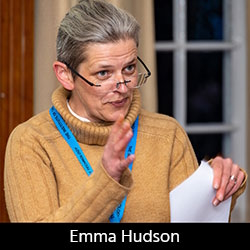
A multitude of delegates from the UK printed circuit industry made the journey to the Institute of Circuit Technology Christmas Seminar on December 5 at the grandiose Majestic Hotel in the picturesque spa town of Harrogate in North Yorkshire. They were welcomed by ICT Chair Emma Hudson, who introduced a program of three presentations encompassing the diverse topics of satellites, electroless metallisation and electronics manufacturing initiatives. |
 |
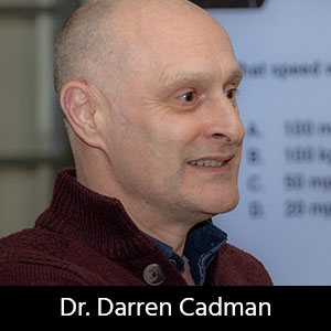
“The next industrial revolution isn’t on Earth” is the tagline for Space Forge, a British aerospace manufacturing company developing fully reusable satellites designed to take maximum advantage of the unique environmental benefits of space in manufacturing next-generation super-materials. Darren Cadman introduced the company and its strategy. He described Space Forge as Europe's fastest-growing space-tech start-up, with funding from the UK Space Agency and the European Space Agency, together with several international investors. The company’s objective is to establish a microgravity research center to drive advanced material research and production, primarily focused on growing defect-free inorganic crystal structures in microgravity conditions for use in electronics. The huge demand for such a service is currently not being met. Not only is there a heavy reliance on the International Space Station but there is a lack of both a dedicated platform and a cost-effective soft-return mechanism. The key attribute of Space Forge is its world-first reusable, returnable orbital manufacturing platform, with its patented system to enable re-entry without burning up and a subsequent soft landing to protect fragile payloads, while reducing stress on the vehicle and minimizing the cost of refurbishment in preparation for re-launch. Cadman explained that in-space manufacturing offers unique environmental benefits that can facilitate the creation of large, near-perfect crystals by chemical vapor deposition and enable the production of semiconductor products with performance superior to anything that can be achieved on Earth, where defects can result from gravity, causing buoyancy effects and preventing perfect mixing of gases, solutions or alloys of different densities. Furthermore, atmospheric contamination issues are avoided in space, where ambient pressure is 10 trillion times lower, and temperatures close to absolute zero can be achieved by radiators facing cold space with no need for cryogenics. The Space Forge manufacturing platform is designed to be launched to a low-Earth orbit at a height of 550 km, with a three-month operational phase followed by a precision de-orbit and recovery from the sea, then taken back to base for inspection of vehicle and payload, refurbishment, and return to service. The system has the potential to prevent the generation at least 15 tons of carbon dioxide for every kilogram of semiconductor material produced for next-generation electronics, telecommunications and automotive applications. |
 |
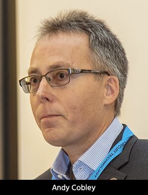
Next to speak was Andy Cobley, professor of electrochemical deposition and leader of the functional materials research group at Coventry University, discussing the development of non-noble metal activators for electroless plating processes, in a project carried out in collaboration with Université de Mons in Belgium. Reviewing the history of electroless copper plating in the electronics industry, Professor Cobley commented that its capability to metallise non-conductive materials has established it as an enabling technology in printed circuit manufacture and latterly in the rapidly evolving field of electronic textiles. Electroless deposition requires the non-conductive surface to first be treated with a “catalyst,” an activator that initiates the redox reaction whereby copper is reduced from the ionic state in solution and deposited on the surface as metal. Formaldehyde is typically used as the reducing agent, and subsequent deposition of copper proceeds autocatalytically. The catalyst of choice has traditionally been colloidal palladium. But palladium is scarce, much in demand, and currently priced at more than £25,000 per kilogram, justifying the evaluation of lower-cost alternatives. Using palladium as a baseline, screening tests were carried out on three candidate materials: titanium dioxide, zinc powder, and cobalt powder. A polyester textile was used as the substrate. Professor Cobley explained the experimental procedure and summarized the results in terms of the effects of concentration, immersion time, temperature, dispersion method, and particle size. He used a series of SEM micrographs to illustrate the physical differences in deposit characteristics. It was observed that both zinc and cobalt could initiate the electroless copper process, and the dispersion method and particle size has significant effects on the final properties of the copper deposit. However, the initiation mechanism was found to be different from that of palladium, since neither zinc nor cobalt showed any catalytic activity. In contrast, palladium acted as the catalyst in oxidizing formaldehyde resulting in copper from solution being reduced to form the initial metal deposit upon which subsequent copper was deposited by autocatalytic reduction. In the case of zinc and cobalt, the initial copper deposit was formed by a simple displacement reaction by a metal lower down in the electrochemical series. |
 |
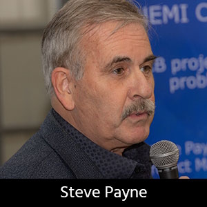
The final presentation came from Steve Payne, project manager at iNEMI, the international electronics manufacturing initiative with a mission to be the premier collaboration forum to forecast and accelerate improvements in the electronics manufacturing industry. He explained the structure of iNEMI, its high-profile global membership, and how its roadmap identifies, forecasts, and prioritizes the future technology requirements, evolution, and infrastructure of the global electronics manufacturing industry in terms of applications and market drivers, technical needs, maturity of technical solutions and expected gaps and challenges—all with a 10-year outlook. He described how individual roadmap teams focus on the full lifecycle and ecosystem of a product, from design through manufacturing and operation to end-of-life, leveraging resources across the supply chain and collaborating to address common industry knowledge gaps. Payne reviewed the portfolio of current iNEMI projects, highlighting those with particular relevance to printed circuit fabrication issues, and described in some detail the work on reliability and loss properties of copper foils for 5G applications, with particular reference to the surface treatment processes used to improve adhesion to resin systems and their effect on signal loss and integrity at high frequencies. Specific objectives were to: Determine and characterize the best non-contact method for measuring the surface topography of very-low-profile copper foil finishes 1. Establish consistency in specifying surface topology of copper foil and bonding treatments
Electrodeposited and rolled-annealed foils were included in the program. Payne briefly discussed non-contact roughness measurement and explained the different parameters: Sa: Representing average surface roughness The current phase of this program is the fabrication of microstrip circuits for the correlation of signal loss with surface conductivity. The next step will be reliability testing, looking for better information than could be gained from traditional peel testing. Other current iNEMI projects mentioned by Payne were: PCB characterization for CAF and ECM failure mitigation, hybrid PCBs for next generation applications, and the PCB connector footprint tolerance project. PCB initiatives in development include immersion cooling, embedded components, ultra-HDI challenges, halogen-free laminate flame retardancy challenges, PCB-level optical interconnects, and pad cratering mitigation. Payne’s presentation certainly captured the attention of the audience and initiated an energetic Q&A session, capably moderated by Hudson, which continued through the buffet supper and into the hotel bar, where it metamorphosed into a welcome networking opportunity for PCB people. Pete Starkey, I-Connect007 |
