|
The Journal of |
| Section 1 | Editors Introduction |
|
Richard Wood-Roe |
In this issue of The Journal our first paper is from Isola. This outlines the developments of pcb laminates in readiness for high frequency 6G communication. Our second paper reviews the development of solder mask properties and challenges leading to todays trend toward additive manufacturing. Finally we have a paper outlining the research into microvia reliability and the effect of high and low resin areas located around the microvia. There is a big change at the ICT as our Technical Director for 20 years, Bill Wilkie, is semi-retiring to become our Chairman. Please read the superb tribute that Pete Starkey has provided in the Members Section. We sadly say goodbye to Dennis Price. One of our industry legends. We have an excellent review of our spring symposium at Meriden. I have found a generous amount of items to add to the industry and membership news sections. I hope you find the contents of the Journal interesting. I welcome your comments or input for the next edition. |
| Go back to Contents |
| Section 2 | Calendar of Events | |
Bill Wilkie |
2024 |
Details |
| March 5th |
ICT Spring Seminar and AGM on 5th March 2024 At the Manor Hotel, Meriden The AGM this year involves the election of a Chairman and Vice Chair. Nominations are invited for these posts and also for the election of new Council Members. |
|
| April 15-18th |
Annual Foundation Course on 15th 18th April 2024 The Foundation Course will be held at Chester University, with the first day hosted by the Merlin Group at their Deeside facility. |
|
| Go back to Contents | ||
| Section 3 |
5G is Setting Stage for 6G Fandy Wei, Senior Director, OEM Marketing in Asia, Isola Asia Pacific (Taiwan) Inc. |
|
It seems like only yesterday, but Fifth Generation (5G) cellular networks have been making wireless connections for almost five years. Already, some of the major carriers and test-equipment developers are looking ahead to around 2029 or 2030 and the expected start of Sixth Generation (6G) networks. Still, 5G has room for expansion, especially at higher frequencies, and it may be in the design and development of that “upper-frequency half” of 5G networks that much can be learned to prepare for 6G. The part of the 5G New Radio (NR) standard developed by the international Third Generation Partnership Program (3GPP) technical standards committee that is so familiar to most 5G users refers to frequency range FR1 from 410 to 7125 MHz and its use of those terrestrial frequency bands has proven efficient and effective. But the many futuristic features that will set 5G apart from 4G, including blazing data rates and video streaming without delays, will be provided by 5G’s higher FR2 frequency range from 24.25 to 71.00 GHz typically using smaller cells placed closely together to overcome the propagation limits of higher-frequency signals. The large 5G FR2 bandwidth available at millimeter-wave frequencies is expected to be exhausted before 6G is commercially available, with users finding many new applications for 5G networks in the forms of Internet of Things (IoT) sensors, control of unmanned vehicles, even connectivity to “self-driving” autonomous vehicles, with mobile video conferencing becoming a standard practice as businesses continue to abandon traditional “fixed” workplaces. To exceed the performance levels established by 5G networks, telecom providers are estimating 6G data rates many times that of 5G, as fast as 95 Gb/s. Such high-speed data rates require large channel bandwidths, which are available at higher frequencies. Those higher frequencies with their wider bandwidths will enable applications as of yet unavailable, such as streaming of real-time data and imaging with less than 1 μs latency for medical procedures and operations where a patient is remote from a surgeon, or the use of virtual reality (VR) and augmented reality (AR) to enable three-dimensional meetings and conferences in which no one is present. Some 6G prognosticators are pointing to frequency spectrum to the upper limits of the millimeter-wave range, from 30 to 300 GHz, or even to the Terahertz range of 0.3 to 3 THz (300 to 3000 GHz). Circuit materials capable of supporting millimeter-wave circuits are currently available, for essential 5G components such as array antennas and filters. But the THz frequency range is still largely the realm of medical imaging and other scientific researchers. Significant advances in conductive and dielectric materials will be needed to support the micrometer-dimensioned transmission lines needed for THz circuits. The opportunity to learn more about those 6G circuit requirements is right now, with the FR2 buildup of 5G network infrastructure. By understanding how circuit materials respond to the needs of millimeter-wave circuit design, those lessons can guide the development of circuit materials with the characteristics needed for 6G systems. Circuit materials such as I-Tera®MT40, Astra® MT77, and Tachyon® 100G from Isola Group exhibit the traits needed for 5G’s FR2 region and even beyond 100 GHz, with minimal loss and excellent dimensional stability. These reliable circuit materials maintain high dimensional stability with temperature, minimizing the ill-effects of temperature during normal operation and during manufacturing processes, such as soldering. All three circuit materials are noteworthy for their good high-temperature durability, characterized by a glass transition temperature (Tg) of +200°C. The materials absorb very little moisture and so will suffer only minimal degradation in performance even under high-humidity operating conditions. These three high-performance circuit materials are examples of the materials being used to assemble printed-circuit boards (PCBs) for the FR2 millimeter-wave frequency range of 5G networks. At those frequencies, the low loss and minimal distortion afforded to those circuits is making possible wireless communications within a part of the frequency spectrum once thought impractical for commercial use. Those same three circuit materials also provide realistic foundations for high-speed-digital (HSD) circuits, since the electronic modules within 5G small cells often involve mixed-signal combinations of high-frequency analog circuits and HSD circuits. Exploring how these circuit materials will respond to the needs of 5G networks operating within their FR2 frequency bands will provide useful lessons for the even higher frequencies and performance goals of 6G networks when they come. It may seem like only yesterday, but technical advances have ways of creeping up quickly. by Fandy Wei, Senior Director, OEM Marketing in Asia, Isola Asia Pacific (Taiwan) Inc. https://www.isola-group.com/news/5g-is-setting-stage-for-6g/ |
|
| Go back to Contents |
| Section 4 |
Recent Developments in Advanced Polymeric Materials for Solder Mask Application: Progress and Challenges William Yung Ling Lim a, Mariatti Jaafar a, *, Ku Marsilla Ku Ishak a, Karuna Chinniah b, Wooi Keong Chan b |
|||||||||||||||||||||||||||||||||||||||||||
|
Abstract 1. Introduction
Among the most pronounced advantages of SM coatings are the prevention of solder bridge and cold solder formation, circuit corrosion, external mechanical stress, and the attachment of the right amount of solder to the copper pad [5e8]. In the current industry, SMs are available in various distinct hues for different applications. They are conventionally distinguished with a green surface in PCBs owing to better visual identification (better contrast) [9]. Black and blue-coloured SMs are produced by adding electrically conductive cobalt and carbon, aimed at shielding from external signals, but these are prone to short circuits. Red is also a popular colour for SMs in PCB prototypes. This is attributable to its good contrast, but it falls short of the popular green colour. Another notable colour, white-coloured SMs, has been widely employed for light-emitting diode (LED) applications due to its higher light reflectance [10]. Apart from the variation of colours, dissimilar surfaced SM types, such as glossy and matte surfaced SMs, are also accessible in the industry. Some studies have found that rough matte surfaced SMs are favoured due to the higher surface roughness that improves the wetting of solder flux in the solder mask defined copper pad, resulting in lower macro voids in the solder joint and, thus, better mechanical reliability of the solder joint [11,12]. On the contrary, matte-surfaced SMs are reported to facilitate more moisture build-up that may cause corrosion issues to components and PCBs [13], which is undesirable in high temperature and humidity applications.
This developmental trend ultimately necessitates the conventional photoimageable SMs to possess greater toughness for better crack resistance at high temperatures, to prevent short circuits or solder bridges, and to provide higher printing accuracy that is limited to the process capability of the screen printing process and the usage of suitable fillers [16,20,21]. 1.1. Classification of solder masks Based on the different manufacturing processes, SMs can be categorised into thermosetting solder masks, ultraviolet (UV) cured solder masks, photoimageable solder masks, and dry film solder masks (DFSM) [22,23]. Thermosetting solder masks, also known as epoxy liquids, are widely utilised in one or two-part curing formulations due to their low cost. The process is also practical and simple, whereby an epoxy liquid is usually silkscreened onto the substrate before thermal curing. It was reported that UV-cured SMs have begun to replace the thermosetting SMs due to their fast curing times, mere minutes compared to hours for the heat-cured SMs [24]. However, there are disadvantages to using UV curing, such as a low degree of curing which results in a lack of adhesion [25]. When a thick coating is cured with a UV source, there is a tendency for certain shaded areas to be unilluminated, and this is contributes to a lack of curing [26].
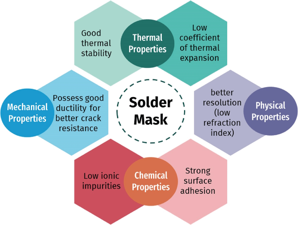
1.2. Ideal characteristics of solder masks As the requirements of electronic components and PCBs are becoming more stringent, it is inevitable that SMs are required to have improved characteristics compared to the past. According to Okada & Toko [33], it is necessary for an SM to have better resolution in the denser semiconductor packages, enabling the solder resist opening (SRO) to be smaller. Therefore, a low refractive index is preferable for a photoimageable SM due to the lack of light scattering during UV curing, thereby allowing the SRO to downsize [20]. In short, the ideal properties of SM are low refractive index, low CTE, high thermal stability, low ionic impurities, good surface adhesion with other materials, and good crack resistance, as demonstrated in Fig. 4. However, the authors remind that certain factors produce an antagonistic effect on each other. An optimum result can be obtained by honing the formulations, material choices and fabrication, deposition, and curing methods.
2.1. Deposition methods for photoimageable solder masks The deposition of LPiSMs can be classified by direct deposition techniques and indirect deposition techniques. The direct deposition techniques include methods that directly deposit a liquid SM onto the desired areas of the non-conductive parts of the substrate (FR-4) without any process for removal from the conductive portions of the substrate (copper traces). Indirect deposition techniques of liquid photoimageable SMs refer to the application of a liquid SM onto the whole surface of the substrate and then removal process of the uncured SM (etching) using a developer solution such as an organic solvent or alkaline solution, depending on the functional groups present that determine the solubility. The selection of the deposition method of liquid photoimageable SM is crucial, specifically for package-level SMs because the resolution, the registration accuracy, and, most importantly, the production efficiency and costs will be greatly affected. Table 1 compares the types of published deposition methods for LPiSM. Photolithography is the typical exposure technique for the indirect deposition methods. It utilises a photomask to transfer a pattern onto the SM to be selectively UV gelled and developed. With a concept similar to photolithography, Laser direct imaging LDI is a more advanced exposure method whereby a digitally saved mask pattern replaces the traditional physical photomask [69]. This maskless exposure method enables cost saving and the lengthy process of creating patterns on the photomask, especially in different circuit designs that require more photomasks. Besides, the LDI process is in tune with the existing photolithography-based deposition methods, providing an easier switch without many changes to the parameters. Better registration accuracy and resolution can also be obtained from off-contact imaging, which is suitable for applying SM in between fine copper traces [67]. With the advent of HDI, LDI has been put out as a solution to the resolution requirement of less than 75 mm consistently [14,63,67]. However, the LDI process comes with a high price tag, and it does not remove the use of developing solutions and the photolithography process, which complicates the fabrication of SMs. 2.2.2. Direct deposition method for LPiSMs Ink-jet printing has the greatest potential in unlocking the higher resolution and registration accuracy of SMs due to the advantages that surpass other deposition methods. One of the advantages is that it is a direct deposition method or an additive manufacturing method, which saves equipment, material costs, and production time without going through the tedious photolithography procedures required in photoimageable SMs [73,74]. Using computer-aided manufacturing (CAM) software, an SM can be deposited through a nozzle onto the substrate in continuous inkjet (CIJ) mode or a drop-on-demand (DOD) mode. The CIJ mode produces continuous ink droplets which are steered through an electric field, and the resulting charged droplets are directed towards the substrate. The more frequently utilised DOD mode produces discrete ink droplets that are ejected through the nozzle by creating pressure waves that overcome the surface tension that holds the ink at the inner nozzle surface [71,75]. These pressure waves in the DOD mode can be categorised into thermal or piezoelectric methods. Thermal methods utilise a thermal heater that generates pressure waves through the formation and disintegration of air bubbles. In contrast, piezoelectric methods deploy a piezoelectric actuator that initiates mechanical movements [65,66]. Recently, this method has become more trending due to its advantages such as high resolution, registration accuracy, and less material waste [23,42,46,66]. The implementation of ink-jet printing removes the need for organic developer solutions and the development of alkali or water-soluble groups for photolithography purposes. Despite that, the jetting of the SM ink can be very complicated at the initial stages. This is ascribable to the high viscosity from the largely shear thinning and thixotropy behaviour of the SM ink [42].
Table 1 Summary of the deposition methods for LPiSM.
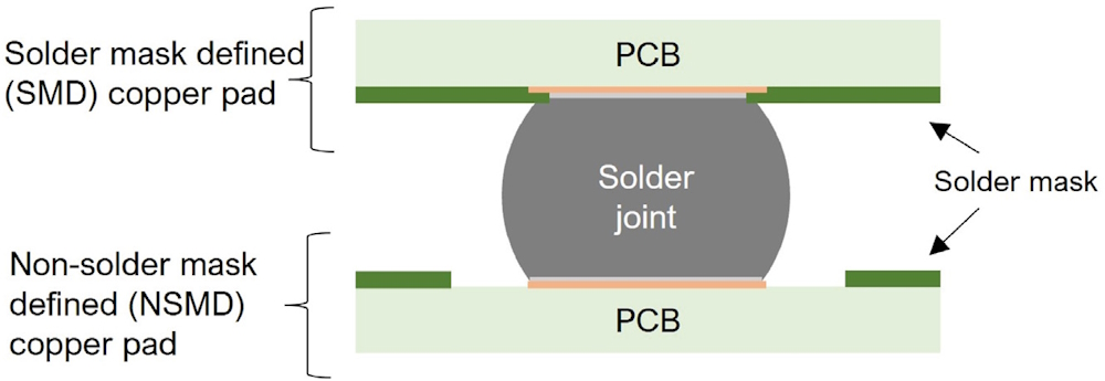
2.3. Curing methods of solder masks Thus far, three notable methods exist to cure SM materials, specifically thermal, UV, or dual curing. Historically, thermal curing has been used to cure epoxy-based SMs. However, the curing times are too slow, resulting in a low production yield [25]. Aside from that, thermal curing requires a very high temperature for hours, which tends to consume more energy. These shortcomings were resolved by UV curing, where fast curing and less extreme temperatures can be practised [78]. Nonetheless, in recent years, there have been ample findings on the need for deep and even curing [79]. This difficulty in obtaining deep curing can cause low crosslinking levels and low Tg SMs, thus producing high CTE SMs that are susceptible to crack generation [80]. While the thermal curing system is as straightforward as the name suggests, two approaches are mainly employed for the UV curing system. Depending on the type of photoinitiator used, an SM can be cured in free-radical photo-polymerisation or cationic photo-polymerisation, which differ in the chemical reaction upon irradiation by UV light [81]. Free-radical photoinitiators produce free radical species through type I photo cleavage or type II hydrogen abstraction reactions from other molecules [82]. Commonly, this system contains an acrylate-based photopolymer and a monomer with a benzophenone, xanthone, or quinone-based photoinitiator [83]. The advantages of a free-radical curing system are fast curing speed, low cost, and ease of preparation compared to ionic photo-curing systems. However, it suffers from oxygen inhibition, which can suppress the degree of cross-linking and thus give poorer mechanical, thermal, and chemical properties [84,85]. Mainstream issues pertaining to photoimageable SMs that led to electrical failure in semiconductor packages and PCBs include SM cracking, ECM, delamination of the SM interface, poor resolution, and undercut, as compiled in Table 6. For package-level SMs, SM cracking is attributed to the mismatch of the CTEs between package materials and the SM coating material. When the PCB is subjected to high temperatures during the assembly or the application, the thermal cycles can generate stress on the semiconductor package materials. The induced stress is distributed to the SM in the form of elastic and viscous strain according to the tan d value of the SM. If high elastic strain exceeds the interfacial free energy of the weakest bonding force in the SM materials, it can cause an SM to be unable to sustain these stresses, thus releasing these energies in the form of cracks [17,34,37,92,93]. Meanwhile, for PCB-level SMs, Coppola et al. [94] reported that upon cooling from the thermal cycles generated from the soldering treatment, the SM coating became brittle due to over-crosslinking and thermal degradation. 2.5. Influence of surface finish and soldering process on photoimageable solder masks For package-level SMs, such as in the flip chip ball grid array (FCBGA) package, SMs are formulated and mixed before being applied onto the surface of the copper-clad laminate using coating or printing techniques. After the deposition step, SMs are cured into a gel form using thermal, UV, or dual curing (UV and thermal) techniques. Later, SMs are developed using organic solvents before the post-cure process. Then, the surface finish to the copper pads is implemented, such as an organic solderability preservative (OSP), metallic preservative immersion tin (iSn), electroless nickel immersion gold (ENIG), electroless nickel electroless palladium immersion gold (ENEPIG) [102]. Lastly, the solder paste is stencil printed onto the finished copper pads of the package and then heated in a reflow oven [103]. Similarly, in PCB level SMs, the manufacturing process proceeds in the same way but with an additional step, where the electronic components are mounted onto the solder paste before a reflow soldering process to melt and harden the solder interconnects [104]. 2.5.1. Surface finishing process 2.5.1.1. Hot Air Solder Levelling (HASL). Among all types of surface finishes, the HASL surface finish for PCB copper pads has been frequently practised due to the cheap cost and the mature technology [107]. In the HASL process, the PCB with cured SM is put into a molten tin/lead solder bath while removing the additional solder through hot air to form a thin copper/tin (Cu6Sn5) intermetallic compound [107]. Pauls [108] proclaimed that ECM might occur when a low thermal stability SM is applied that entraps the water soluble solder flux. Hence, the SM must be formulated to obtain thermal properties that can sustain HASL treatment. 2.5.1.2. Organic solderability preservative (OSP). Another economical alternative to HASL is OSP, which is one of the most utilised surface finishes. It is a facile process and space-saving but is said to have poor corrosion resistance, resulting in a need for an inert nitrogen atmosphere during solder reflow [96]. OSP is based on organic azole molecules that form a surface finish film in the form of copper complexes [111]. This surface finish necessitates the adjustment of pH and the minimisation of contamination through acid cleaning with acetic acid, water rinsing, and micro-etching by hydrogen peroxide. Nichols and Carano [96,112] described the overall process flow of OSP. It was reported that OSP residues formed from benzimidazole's evaporation could contaminate the surface of the SM and lower its surface energy [49]. Hence, an SM with much improved thermal properties is required to withstand OSP influences. 2.5.1.3. Electroless nickel immersion gold (ENIG). Meanwhile, the key steps of ENIG include surface cleaning with acid, etching, activator treatment, electroless nickel plating, and gold immersion plating processes. The overall process may modify the SM surface chemistry due to the presence of acid in the cleaning step and the high thermal conditions in the plating and immersion steps [113]. Recent publications suggest that SM dissolution occurred during the ENIG process. This will interfere with the nickel plating step and generate surface defects such as black pad [106,114]. 2.5.1.4. Tin immersion (iSn). The effect of an iSn surface finish on SM properties has also been investigated by Hofmeister et al. [49], whereby iSn residues formed from soldering treatment accumulated on the SM surface, which diminished the surface energy of the cured SM. Although the highest temperature encountered, up to 75oC, was outlined to be in the immersion tin step, it was reported that volatiles in the SM can evaporate and condense on the Sn surface, which creates a reliability issue [115]. An overview of the surface finish on SMs is compiled in Table 2. Table 2. Overview of Surface Finishes of Solder Mask
2.5.2. Soldering process
3. Advanced solder mask materials As opposed to the typical epoxy acrylate-based photoimageable SM, several efforts have focused on developing the microstructure of an SM towards its ideal characteristics and preventing typical SM issues. Attention has been growing on alternatives to organic solvents and on using materials such as polysiloxane, hyperbranched polymers, et cetera as the main materials to combat issues such as mitigating the brittleness of typical epoxy-based SM. 3.1. Development of alkaline-soluble and water-soluble groups With the spread of environmental awareness these days, there have been concerns regarding the utilisation of harmful organic solvents in the SM formulations and the developer solutions. To minimise the evaporation of these harmful volatile organic compounds (VOC), alkaline soluble SMs have been developed. The reaction between epoxy and acrylic acid produces hydroxyl groups which then form alkaline soluble carboxyl groups upon reaction with an anhydride hardener. Further addition of dicyclopentadiene resin to the SM provides the lowest viscosity for longer pot life and the highest resolution, up to 40 µm, on an epoxy glass fibre substrate, which fulfils the tight tolerance of SRO. In contrast, adding an isocyanurate type epoxy to the SM can allow it to withstand a soldering process at 260oC for 30 s and three cycles without losing adhesion [50]. 3.2. Introduction of a siloxane backbone chain 3.3. Introduction of hyperbranched polymer and reactive diluents The ink-jet printing deposition method and application of SM in FPCB necessitates the SMs to have reduced viscosity apart from decreased brittleness. Several means of toughening methods are well-known to mitigate brittleness, such as adding elastomers, specialty thermoplastics, and nanomaterials. However, there are limitations such as high costs, processing difficulties, and poorer thermo-mechanical strength. This has prompted the emergence of hyperbranched polymer [123]. In 2015, Yang, Chang & Yang [42] synthesised hyperbranched polyester epoxies (HBPEs) and hyper-branched polyester epoxy acrylates (HBPEAs). HBPEs were found to have lower initial curing temperature and activation energy while also achieving better resolution than commercial epoxy resins with the same amount of hardener. This is due to the less shear thinning behaviour and high functionality of hyperbranched polymers compared to linear polymers, which resulted in a curing reaction before spreading. Meanwhile, HBPE and HBPEA also showed reduced weight loss in the thermal gravimetric analysis (TGA) test. There has been no investigation of the mechanical properties of hyperbranched polyesters in SMs yet. Nevertheless, it is predicted that a high amount of branching will give rise to high free volume content, which improves the ductility but lowers the Tg as any toughening agent would. Meanwhile, due to their lower toxicity, plasticising effect, and enhanced ductility from their reaction in the curing process, reactive diluents were also utilised in place of organic solvents This work outlines a summary of the importance of SMs based on the current demands of the electronic industry and recent publications. Different SMs were also categorised, and the ideal characteristics of SMs were discussed, where an SM requires optimisation of material formulations to achieve the optimum results. Besides, the topic of photoimageable SMs and the influence of SM related manufacturing processes on their properties was extensively reviewed. As the requirements for SMs have become uncompromising, more photoimageable SMs were developed towards polymer composite formulations, which are favourable in reducing SM's CTE level. To tackle some of the issues of photoimageable SMs, advanced SM materials have been synthesised through modifications of SM microstructure, such as introducing water soluble groups for development, siloxane polymers, hyper-branched polymers, and reactive diluents. These have tremendous prospects for fulling the ever-growing needs of the electronic industry. Declaration of competing interest The authors declare that they have no known competing financial interests or personal relationships that could have appeared to influence the work reported in this paper. Acknowledgments The original paper and supporting references can be accessed rom this link https://www.sciencedirect.com/science/article/pii/S2468217923000369 This work was supported by Micron Memory Malaysia Sdn Bhd through the External Research Grant (Grant no. 6050503) as well as to School of Materials and Mineral Engineering Resources Engineering, Universiti Sains Malaysia, for their financial and technical support. © 2023 Vietnam National University, Hanoi. Published by Elsevier B.V. This is an open access article under the CC BY-NC-ND license (http://creativecommons.org/licenses/by-nc-nd/4.0/). |
||||||||||||||||||||||||||||||||||||||||||||
| Go back to Contents |
| Section 5 |
Influence of Substrate on Microvia Structures in Printed Circuit Boards During Reflow Syed Mujahid Abbas1, Qiang Yu1, and Michael Pecht2, (Life Fellow, IEEE) |
|
Abstract Index Terms Finite element analysis, microvia, printed circuit board, reflow, reliability, substrates, Taguchi method.
With the sudden increase of features in the automotive industry, the demand has grown for compact PCBs with higher densities of components and their reliability concerns. For example, flame retardant (FR4) is the most used PCB laminate material that presents a major reliability concern because of its large coefficient of thermal expansion (CTE) in the thickness direction of PCBs [8], [9]. As miniaturization advances, it is thought that several factors significantly influence PCB reliability. These factors include the effect of via diameter, aspect ratio [10], [11], [12], [13], [14], [15], and the plating thickness of PCBs [16]. Therefore, to optimize the design margin for miniaturization, FR4 was treated as a homogenous body, averaging out the collective impact on microvias. FR4 is typically a composite in which plain fiberglass woven cloth and resin are laminated [17]. The microvia is made using the drilling process and most of the surrounding area is glass fiber and resin [18]. No studies have been conducted on finding the interaction between microvia and its immediate surroundings. Figure 1 shows a schematic diagram of a single-layer PCB substrate with different fiber and resin concentrations across the board. Microvia reliability research has primarily centered around the core focuses of design optimization and understanding the failure mechanisms of microvias. Some researchers have focused on experimental investigations of the reliability of single level microvias [19], [20]. Some publications have addressed the microvia reliability of single level unfilled or epoxy-filled microvias. However, few researchers have addressed the reliability of copper-filled microvias [21], [22]. Recent research found that concentration of small elements in electroless copper of microvia affects the reliability of HDI substrates [23], [24]. Birch [25] tested stacked electroplated microvias and found that two-level stacked microvias are relatively more reliable than four-level stacked microvias. Previous research has found different types of failure in microvias including cracks around corners, knees, pads, and interfacial separation [19], [20], [21]. Ning et al. [26] investigated the voiding effect on the reliability of copper-filled stacked microvias in detail with different characteristics of voiding such as void shapes, location, and sizes. However, previous studies did not investigate the substrate layer’s influence on microvia structures. In reliability investigations, it is easy to control individual variables in numerical simulations, but evaluating the combined effects of factors poses challenges. The Taguchi method invented by Japanese scientist Dr. Genichi Taguchi addresses this issue by providing the assessment of combined factors and their impact on product reliability through a reduced number of simulations. The Taguchi method focuses on the effective application of engineering strategies instead of advanced-level statistical techniques and is widely used in the design of experiments (DOE) [27], [28], [29], [30]. The reliability of microvias in automobile PCBs is crucial. Automotive PCBs more often need to survive in severe environments than other applications and demand robust microvia interconnections to reduce failure-related costs. Thus, the automotive industry requires ensuring a zero-failure rate from microvia reliability. Additionally, the large number of microvias makes it impractical to test each microvia of PCB lots due to time and cost constraints. Previous studies that regard substrates as uniform fail to capture the real-time impact of substrates on microvias. Therefore, there is a need to figure out the real impact of the composite substrate on microvias during reflow. In this paper, a comprehensive composite finite element model is developed to research the intricate dynamics of substrate layers and their influence on microvias. By utilizing the DOE technique using the Taguchi method, this paper explores critical factors affecting microvia failure above glass transition temperatures. The authors found that uneven distribution of resin and fiber in the substrate resulted in different stress concentrations on microvias. This research presents a major contribution to understanding the behavior of composite substrates and provides valuable insights for optimizing microvia reliability in automotive PCBs. The rest of the paper is organized as follows. The novel approach of this research is described in Section 2. Finite element modeling details are presented in Section 3. After the Taguchi methodology with the proposed factors has been described in Section 4, Section 5 presents the simulation results. Section 6 presents the different characterized failure risk areas for microvias. Section 7 is the discussion and Section 8 concludes the paper. 2. Novel Approach
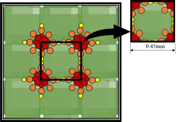
Therefore, it is necessary to determine the areas across the substrate where a high possibility of microvias failure exists. Fiberglass cloth has low CTE while epoxy resin has high CTE. The substrate throughout the layer consists of resin-rich and fiber-rich sites. So, the entire PCB does not carry an equal risk of microvia failure. Furthermore, the stress concentration of microvias in different positions on PCB yields varying results due to irregular distributions of fiber and resin as shown in Figure 2.
Fig 2. Illustration of microvias at various positions in different fiber resin concentrations.
3. Finite Element Modelling Due to impregnation, the resin layer in between the fiber bodies is negligibly small and is not considered in modeling. However, the effect of resin is accounted for through the material properties, which adhere to the composite rule of mixtures, ensuring balanced characteristics. For microvia modeling, both capture and target pad diameters are 200 µm, microvia diameter from the capture pad end is 110 µm and from target pad end is 100 µm. The height of microvia is 100 µm. Figure 3 shows the finite element analysis model of woven fiberglass with microvia interconnect. The fiberglass and microvias are encased within a resin layer.
Fig 3. Finite element model of FR4 substrate including the model of microvia.
The glass fiber cloth has a single layer in which threads are woven in X and Z direction. Figure 4 shows the illustration of fiber cloth with design parameters that were considered for the finite element modeling of fiberglass 1 and 2. The detailed dimensional measurements of glass cloth are shown in Table 1. The fibreglass is an orthotropic material with two directions (i.e., X and Z directions) orthogonal to each other in the board plane and a third direction (Y-direction) out of the plane. In this study, the orthotropic glass fiber material properties were used and are listed in Table 2 [32].
Fig 4. Schematic diagram of glass fiber cloth cross section with design nomenclature.
The equivalent CTE of fiber in X and Y (thickness) has the value of 15 ppm/o since it has a fiber-resin matrix and was used following the composite rules of mixtures. The isotropic resin is supposed to change remarkably above the glass transition temperature Tg of 137oC, listed in Table 3 [33]. The CTE of copper is 17 ppm/o, E = 120 GPa is the elastic modulus, and the Poisson ratio is 0.35 [33]. Finite Element Analysis was conducted for the determination of thermo-mechanical stress evolution in microvias under thermal loading. As for the temperature load, the initial temperature was set at room temperature, 25oC. The temperature load was given in two steps elevated from room temperature i-e., from 25oC to 240oC. The temperature holding time was not considered because the analysis in this study was not an absolute evaluation of strain occurring in microvia and base material. In this study, von Mises stress was observed to determine the location of the potential failure site and maximum damage. The authors measured the equivalent CTE and equivalent Young’s modulus of the composite model. The results were compared with the typical range of FR4 material properties reported in the literature [14], [26], [33] to verify that the results are logical and fair to use. The results are shown in Table 4. 4. Taguchi Methodology
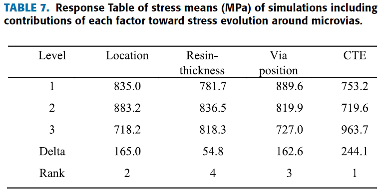
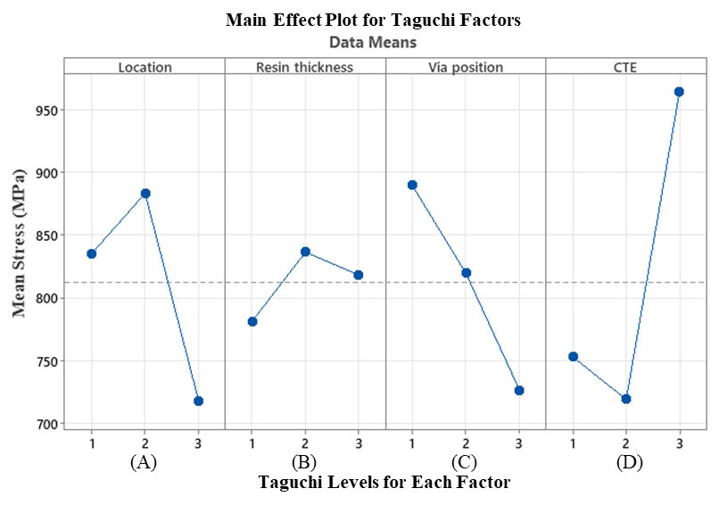
Taguchi factors from A to C, are schematically shown in Figure 5. Factor D is the resin material property i.e., CTE is shown in Table 5. Since the microvia location is the key factor in finding the high-potential failure risk areas, the design factor ‘Via Position’ was also considered. Three via positions were modeled from the center of the resin-rich area as shown in Figure 5(c). Epoxy resin influences PCB with respect to glass transition temperature (Tg) limit (smaller CTE values under Tg and much larger CTE values above Tg) [33]. Three levels of CTE for the Taguchi trial run were established by increment and decrement of original CTE by 10% and are shown in Table 5. The trial run order with corresponding factor and their levels is shown in Table 6.
Table 6. Taguchi L9 (34) orthogonal array with respective values of factors.
5. Results
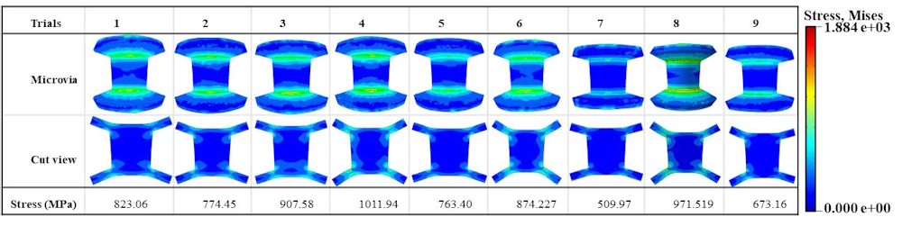
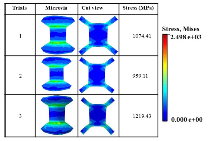
Fig 6. Microvia stress distribution simulation results across substrate models of Taguchi L9 orthogonal array (OA): Blue color indicates minimum stresses whereas red color indicates maximum stresses on microvias. Each microvia model displayed maximum stress concentration at the corners.
Fig 7. Main effects plot for stress means of each Taguchi factor. Y-axis is the same for all result trends i.e., Mean stress. X-axis (A) microvia locations across the substrate (B) resin thickness in µm (C) microvia positions on fixed via locations across substrate in µm (D) coefficient of thermal expansion of the resin in ppm/o.
Fig 8. Simulation results of microvias at open resin window location on the substrate.
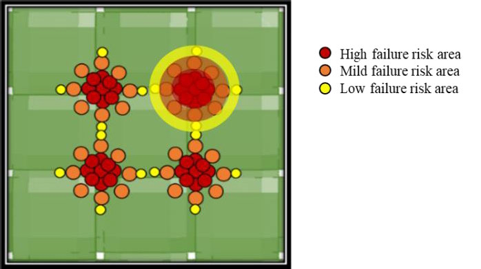
Fig 9, Illustration of microvia failure risk zones from high(red) to low (yellow) risk on the substrate.
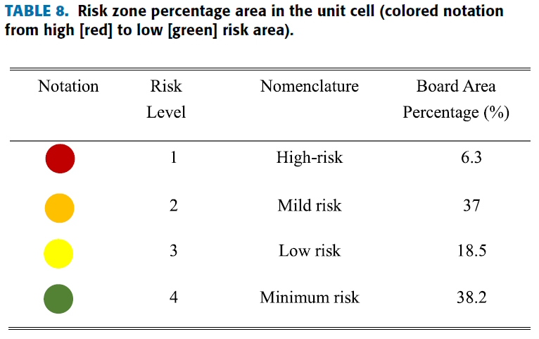
6. Risk Area Calculations
Fig 10. Illustration of the unit cell of the board to calculate risk zones around the cell in percentage.
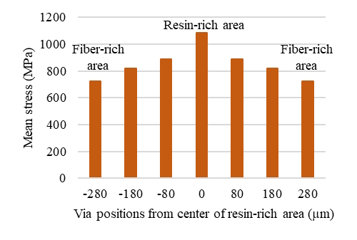
Risk calculations were done statistically based on the risk levels of microvias in the unit cell. Only 6.3% of the area turned out to be a high failure risk area for microvia failure, whereas 38.2% area of the unit cell had a minimal risk for microvia failure. Table 7 shows the details of the calculated percentage of PCB area in a unit cell that possesses high failure risk for microvias. From Table 8, it is evident that the substrate has a very small proportion of the total board area in which microvias demonstrate a high failure rate. Figure 10 shows that the unit cell contains a high failure area on each corner, demonstrating a uniform pattern throughout the PCB. The highest mean stress outcome of 1084MPa was observed at the center of the resin-rich area and moderately decreased when a microvia was positioned at some distance from the center of a resin-rich area as shown in Figure 11.
Fig 11. Mean stress values of microvias in various positions on substrate.
7. Discussion Additionally, the fiber-rich and resin-rich areas of the substrate had a significant impact on the microvia structure. The fiberglass weave bundle strengthened the microvia structure lowering the risk of failures above the glass transition temperature. The microvias at the center of the resin-rich area observed a maximum mean stress concentration of 1084 MPa whereas the microvia at the location of the fiberglass weave observed 727MPa mean stress around the corners (as shown in Figure 11). A 33% increase in the mean stress concentration on microvias was observed that was present in a high failure risk zone, compared to the stress concentration present in a low failure risk zone. Throughout the fiberglass cloth, open resin windows are the locations that have 0% fiber content and 100% resin content. Based on the outcomes shown in Figure 8, open resin window locations of fiberglass have the highest potential failure risk for microvias. However, the area of the high microvia failure-risk zone is too small i.e., only 6.3% of the area in the unit cell contains the high failure site for microvia that might be replaced in design optimization. Additionally, to mitigate failure risks, careful consideration must be given to designing the pitch in a manner that avoids high-risk areas. 8. Conclusion Among all the parameters studied in this work, the thermal expansion coefficient and microvia location have the most significant influence on microvia structures. Specifically, at the center of the open resin window, microvia exhibited the highest stress of 1219.43 MPa among all simulation results. This indicates that the possibility of microvia failure could be increased if microvia is located at the open resin window location of the substrate with high CTE. Therefore, more attention should be given to these two parameters during the designing and testing phase of the HDI boards. The fiberglass weave in the substrate provides strength to the microvia at elevated temperatures and prevents it from early failures. Moreover, recognition of high-risk failure sites can guide design improvements, considering the design parameters such as microvia diameters and pitch to improve reliability during the design phase. References: Please refer to the original document using the following link: https://ieeexplore.ieee.org/document/10359520 Syed Mujahid Abbas received the B.S. degree in mechanical engineering from the University of Wah, Wah Cantt, Pakistan, and the M.S. degree in mechanical engineering from Yokohama National University, Japan, where he is currently pursuing the Ph.D. degree with the Department of Mechanical Engineering, working on the reliability of PCB for his dissertation. His other research interest includes reliability and strength of materials. Qiang Yu received the M.S. and Ph.D. degrees in mechanical Engineering from Yokohama National University, in 1989 and 1992, respectively. He is a Professor with the Department of Mechanical Engineering, Yokohama National University. His main research interests include reliability assessment of electronics equipment and systems and computational engineering. MichaeL Pecht (Life Fellow, IEEE) received the first M.S. degree in electrical engineering and the second M.S. and Ph.D. degrees in engineering mechanics from the University of Wisconsin, Madison, USA. He is the Founder and the Director of the Center for Advanced Life Cycle Engineering (CALCE), University of Maryland, which is funded by over 150 of the world’s leading electronics companies at more than US$6M/year. He is currently a Distinguished Professor in mechanical engineering and a Professor in applied mathematics with the University of Maryland. He is a world-renowned expert in strategic planning, supply chain management, design, testing, IP, and risk assessment of electronic products and systems. He has written more than 40 books on product reliability, development, and supply chain management. He has also written over 900 technical articles and has ten patents. He is a Professional Engineer, an IEEE Fellow, an ASME Fellow, an SAE Fellow, and an IMAPS Fellow. In 2010, he received the IEEE Exceptional Technical Achievement Award for his prognostics and systems health management innovations. He is serving as the Editor-in-Chief for Circuit World. He served as a Chief Editor for Microelectronics Reliability, for 16 years, and IEEE Transactions On Reliability, for nine years. |
|
| Go back to Contents |
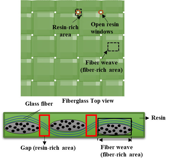 Fig 1. Schematic diagram of the substrate and top view of fiberglass.
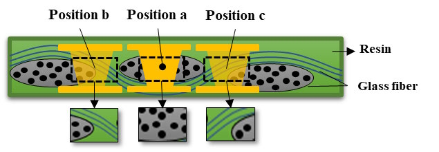
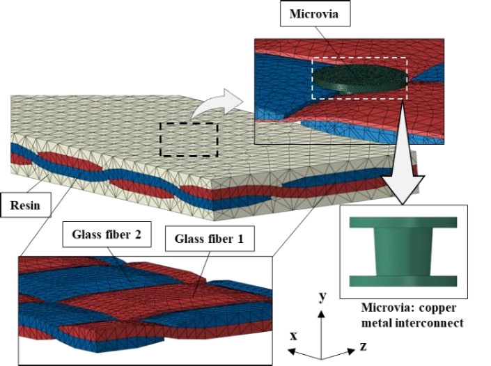
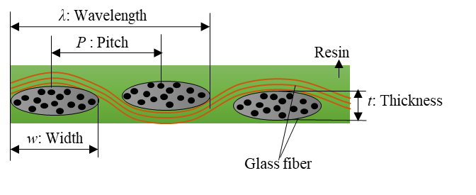
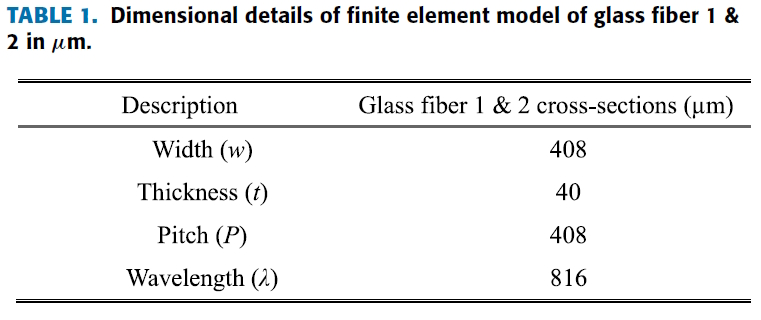
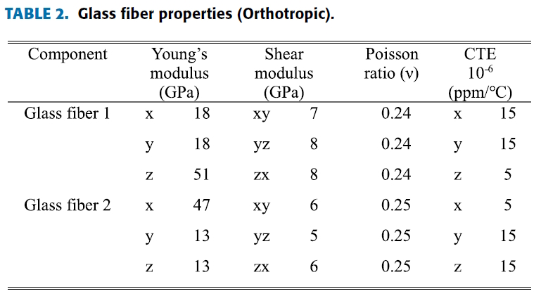
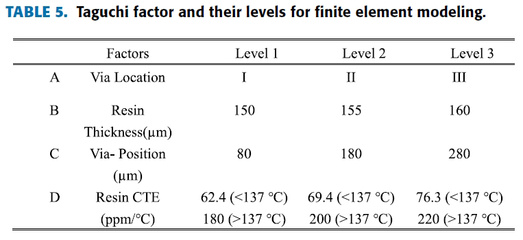
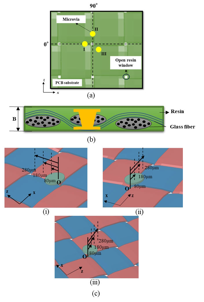 Fig 5. Schematic of Taguchi factors. (a) illustration of Taguchi factor A i.e., microvia locations at PCB substrate (b) Schematic of Taguchi factor B i.e., resin thickness (c) Schematic of Taguchi factor C i.e., via positions on each via location along z(i), along x(ii), and at 45◦ between z and x(iii).
| Section 6 |
The Institute of Circuit Technology Spring Seminar 2024 March 5th 2024, Meriden |
|
Photo Alun Morgan |
Meriden continues to be a popular midlands venue for Institute of Circuit Technology events and some encouraging signs of early springtime were evident as members arrived to attend the Annual General Meeting and to enjoy the 2024 Spring Seminar. The seminar speaker was Alun Morgan, President of EIPC, the European Institute for the PCB Community, who presented a comprehensive analysis of the global electronics industry, a business outlook with an emphasis on Europe and an exploration of some capabilities of Artificial Intelligence. Reflecting on 2023, there had been a rapid expansion of generative AI technology against a background of economic uncertainty and accelerating climate crisis. Post-Covid, massive sums of money had to be reconciled, supply chains had been disrupted and geopolitical tensions had resulted in increasing sanctions and trade controls.But new innovations and opportunities technology were emerging. Artificial intelligence, electric vehicles, automation and robotics, new energy outlooks and aggressive data collection had all made major gains in 2023, although the future held risks in economic, environmental, geopolitical, societal and technological categories. World GDP growth was forecast to reach 2.9% in 2024, from 3.5% in 2022 and 4.0% in 2023, but the Euro area forecast was only 1.0%, from 3.3% in 2022 and 0.7% in 2023. World PCB output for 2023 was estimated at $90,090M, from $91,375M in 2021 and $97,505M in 2022. By comparison, the 2023 estimate for Europe was $1,980M, from $2,025M in 2021 and $2,160M in 2022, and the downward trend in European PCB output appeared to have flattened off. Nakahara had predicted that 2025 will be a good year for the world industry, but commented that this will be heavily influenced by recovery in IC substrates, since they now represent 20% of bare-board output. By contrast with the worldwide figure, Custer’s outlook for Europe expected real GDP growth in the euro area to be around 1% in 2024, and somewhat lower growth was expected for countries like Germany with a high proportion of industrial production Economic growth in the US was expected to be somewhat stronger, partly because the US is less affected by high energy prices than European economies. However, the predicted economic growth in 2024 would only happen if there were no additional effects such as new global supply bottlenecks that could lead to interruptions in production. Geopolitical uncertainties posed a further economic risk, and an escalation of existing conflicts, particularly the war in Ukraine and the conflict in the Gaza Strip, could result in significant supply chain problems and rising commodity prices. Custer considered that if political parties whose policies focused on economic isolation were to prevail in upcoming elections in Europe and the US, there would be negative consequences for all export-oriented economies. And while the biggest economic risk in 2023 had been energy security, political and geopolitical uncertainty would pose the biggest risk in 2024, resulting in declining investment. This would weaken both short-term and long-term growth and employment, and permanently weaken overall economic production capacities. Michael Gasch had made some interesting comments on the European PCB industry. His figures indicated that the German-speaking countries jointly represent the largest share of production, 62% of all Europe, with the Latin countries jointly representing 22%, the UK representing almost 9% and the rest of Europe about 7%. The production percentages related to the industries served in those regions, Germany, Austria and Switzerland being strong in industrial electronics, and Switzerland additionally in medical electronics. France, Italy and UK were heavily engaged in defence, aeronautics and space, and all had a fair share in supplying the EMS industry, for which in most cases no end-use sector could be specifically allocated. The Germany-Austria-Switzerland region had seen a decline of about 5% in its PCB business, while the Latin countries achieved an increase of 16%, the UK an increase of 4% and the Central European countries a slight decline of 7%. On balance, the total for Europe in 2023 was about the same as in 2022 although there was still a lot of uncertainty because of world geopolitical factors. There was some good news! Teltonika, a leading manufacturers of Internet of Things and network connectivity solutions, is investing around 143 million euro in a new PCB factory in Vilnius, Lithuania, covering an area of more than 33,000 square metres and expected to become one of the most advanced of its kind in Europe, with the highest level of automation and meeting the strictest environmental standards. Teltonika aims to complete the project in December 2024. Morgan handed round some examples of their products and commented that, altough this would be a captive shop, it would help to secure the supply chain. Morgan turned his attention to the automotive industry, and listed the world’s top 10 plug-in electric car brands of which the leader by far was the Chinese BYD, with Tesla in second place and European brands quite small in comparison although, as he remarked, still representing an important market opportunity for the PCB industry. He discussed the growth in driver-assistance systems and classified the “levels” for ADAS and autonomous operation. Levels 0 to 4 defined the extent of automation from zero to high: “full attention”, “feet-off”, “hands-off” and “eyes-off” respectively. Full automation, Level 5, was not forecast to be reached before at least 2030. Having delivered a wealth of information and opinion while holding his audience engrossed with his fluent and articulate style, Morgan concluded his presentation with a short discussion of his current favourite topic - Artificial Intelligence. He began by illustrating the response he got from Chat GPT to his question: “Tell me about artificial intelligence usage for printed circuit board design and manufacture” The chatbot replied that AI is increasingly playing a significant role in the field of printed circuit board design and manufacture, and gave him three pages of detailed information under the heading Automated Design Optimisation and sub-headings Topology Optimisation and Routing Optimisation. Further section headings were Generative Design, Predictive Analytics, Automated Testing and Inspection, Supply Chain Optimisation, Machine Learning for Fault Detection, Process Optimisation and Customised Design Assistance. Its summary was that “AI is transforming the PCB deign and manufacturing process by introducing automation, optimisation and predictive capabilities. This not only enhances the efficiency of the design and production phases but also contributes to the creation of more reliable and high-performance electronic devices”. Morgan commented that if he asked the same question at a later date, he received an updated reply, as the chatbot was continously learning and improving its expertise. He ended with a demonstration of how a photograph could be edited, modified and transformed, just by telling the AI system what was required and allowing it to use its creative imagination. “The camera doesn’t lie…” was no longer the case – Morgan explained that in the digital age, an original photograph was effectively only a complicated set of ones and zeros, open to manipulation. He avoided being drawn into a debate about the finer points of copyright! The evening was rounded off with a buffet supper and networking session – the constructive exchange of opinions, experiences and industry gossip that features whenever members of the Institute get together. Many thanks to Bill Wilkie for his organisation of a splendid event. |
| Go back to Contents |
| Section 7 | Obituary Dennis Price |
| Dennis Price |
Dennis Price was a legend. A great family man and fiercely, fiercely proud of his daughter, Susan. He was a countryman, skilled in the art of game shoots and knew both ends of a shotgun better than most. He also had the patience to train several gun dogs and mentor others who were trying to do the same. He also found time to acquire an encyclopaedic knowledge of printed circuit quality standards. I met Dennis in 1980, but his story goes much further back. Indulge me a minute, because his life story is connected to the birth and growth of the pcb industry. It goes back to 1960, when a company called Mills and Rockley were starting to make embryonic pcb’s. Not related, Kenny Mill turned up in in Galashiels in a room above the British linen Bank making those same circuits with Robert (Bert) Currie as Currie and Mills. They grew and split in 1962, with Bert Buying out Kenny, who went on to Start Bepi Circuits in Galashiels – one of the largest manufacturers in the UK. Currie and Mills became Exacta Circuits, first in Netherdale road in Gala and then in a purpose-built facility in Selkirk, in its day the largest facility in the UK. Dennis worked at Mills and Rockley (who became Delta Printed Circuits) in Skelmersdale before joining Dynachem for a short while. He joined MEPD in '78. and that is where I met Dennis. He was there for 15 years before going to Graphic Electronics in Devon. Graphic was owned by Rex Rozario, but their General Manager was a big lad from Fife called Jeff Murphy – a real character. Dennis and Jeff got on really well and when Jeff left to found a buyout of Kemitron at Deeside, Dennis went with him as Quality Director. When Kemitron was bought out by Neil Martin it became part of the Merlin pcb Group, still the largest family run shop in the UK, where Dennis spent the rest of his career. He also found time to be elected a Fellow of the ICT and lectured in Quality standards at both Loughborough University and Chester University on our Annual Foundation Course. Dennis was elected an Honorary Fellow of the Institute on his retirement. At MEPD he took Andrew Brown and I under his wing and tried to teach us the lore of the countryside. We set off on a road trip complete with shotguns and hip flask and ended up at a huge rabbit warren, where we singularly failed to connect with anything other than turfs of grass! We then engaged in Italian shooting with Dennis driving up the middle of a field with Andrew and I in the back seats, shotguns out the rear windows. Still nothing. He took us to a Stand of crows, where we fired in the air to no avail. Ah well, back to the Woodburn. He suffered from an aneurism and was placed in a coma where he remained for months. He couldn’t move at all but could hear what was going on. A discussion was taking place between the surgeons, and he could hear Eileen’s voice. A voice said that they had tried to revive him twice and they could only try once more before they had to switch off the apparatus. He suddenly realised that they were talking about him! The rest is history. Dennis was unique. When they made Dennis, they threw away the mould. He knew those at Mills and Rockley and Currie and Mills and was at Exacta and MEPD, Dynachem, Graphic and Merlin. He encompassed the entire industry and built up an unparalleled knowledge base. It can never happen again. When I joined the ICT in 2004, I was a one-man band in Kelso with aspirations and wondered what it would be like to have a Technical Help line. Enquiries would come in and be farmed out to industry experts around the world. As it happened, Dennis was the only expert we needed and he became the Technical Helpline, assisting us from the bank of filing cabinets in his garage long after retirement! There’s a latin phrase you see often– sic gloria transit – a little bit of the glory of the world has passed away and that was Dennis Price. |
| Go back to Contents |

| Section 8 | Members News | ||||||
|
Welcome, Chairman Bill Wilkie! Speaking as an Institute member since the mid-1970s, and having served on the Council since the late 1990s, I have a reasonable recall of the major events of the last few decades. From the point of view of the Institute, surely the most notable one was the appointment of Bill Wilkie as Technical Director and Membership Secretary back in 2004. From its original inception as a Printed Circuit Group in 1964, followed by its adoption as a division of the Institute of Metal Finishing, then going independent again as the Association of Circuit Technologists, it was eventually incorporated in the mid-1970s as The Institute of Circuit Technology with Doug Taylor as Chairman and established a clear identity at a time when the UK printed circuit industry was booming. The Institute provided a platform for individual engineers involved in printed circuit fabrication, offering a wide range of technical seminars and training opportunities together with professional grading reflecting experience and achievement. It established a membership of over 400. The ICT began to lose its clear identity when it combined with the Printed Circuit Association, which represented the corporate members of the interconnection industry in the UK, to form the Printed Circuit Interconnection Federation. Then, when the PCIF was absorbed into the Federation of the Electronics Industry and its successors, the Institute was virtually lost in the noise – an insignificant minor component of a major trade association. So the ICT became an independent organisation again, although by the turn of the century the UK printed circuit industry was but a shadow of its former self and membership numbers were dwindling. We needed new momentum and a new driver. I had known Bill Wilkie since our days in technical sales at Thiokol-Dynachem. I had moved into PCB manufacturing while Bill had remained in sales and built up a huge network of contacts in the industry. He was enjoying his retirement when the Council of the Institute approached him with a new challenge – would he like to join us on a part-time basis with the objective of consolidating and building the membership? Bill accepted the challenge! In the following twenty years, with the support and encouragement of Council members but largely as a result of his own efforts and commitment, together with the universal respect he has earned from the industry, he has increased the membership to over 400 As Technical Director he has established training courses and education initiatives and has virtually single-handedly organised our seminars and symposia. We have been represented on a number of grant-funded projects. And there are all sorts of additional tasks that Bill has quietly undertaken in the background, that we may be guilty of having overlooked or have taken for granted. The Institute owes a huge debt of gratitude to the contribution that Bill Wilkie has made over the last two decades. What started as a part-time challenge has become a mission with a notable record of successes. Thank you Bill! We respect your decision to retire from the role of Technical Director. You will be a worthy Chairman of the Institute and we wish you every success in that position. Pete Starkey - ICT Council |
|||||||
|
Exception PCB
|
We are delighted to announce the promotion of Conrad Bailey to the new position of Sales Manager. Conrad has worked in the PCB industry for over 30 years and joined Exception PCB Ltd last year. We wish him all the best in his new role. |
||||||
|
Graphic
|
I have embarked on a new chapter in my career, returning to Graphic PLC as Sales and Marketing Director. This is an amazing opportunity for me to rejoin a company that is at the top of its game both technically and commercially. I will head up and support Graphic's amazing sales team, which has been serving the needs of the industry for decades. I look forward to being part of a company that has ambitious plans for the future and an appetite to continuously improve. |
||||||
|
GSPK
|
We are delighted to announce the expansion of our team with the addition of three highly experienced professionals. Les Blakeman - Business Development Manager, Richard Ross - Technical Team and Natalie Crozier - Internal Sales. This strategic move comes on the heels of the unfortunate closure of Faraday Circuits, a respected UK PCB manufacturer. |
||||||
|
Ventec Group
|
We are pleased to announce the appointment of Leigh Eastwood as Technical Sales Engineer. Covering the UK and Western European regions, Leigh will work to bring Ventec’s advanced thermal management and high-speed solutions to a wider audience, providing unparalleled expert-level support to both existing and new customers. Read more... |
||||||
|
|

 Wayne Loshi


|
Industry News |
|
|
Adeon Technologies BV
|
Adeon Technologies have produced a webinar to explore the innovative world of additive manufacturing for PCB solder masks. This webinar includes a live session where the SUSS JETxSM24 will perform a coating. After that, an explanation of the few easy steps needed from design to print will follow. Together with our partners from Adeon Technologies, Agfa-Gevaert and Electra Polymers we will present the qualities of their material and the ESG advantages of additive manufacturing. This webinar will dive into how additive manufacturing accelerates production, reduces waste, and minimizes material and energy consumption, marking a significant advancement in PCB manufacturing. |
|
A-Gas
|
At A-Gas, reflecting on the work we do and celebrating our successes is incredibly important. Looking back at Q1 allows us to think about the progress we've made as a business and how positive the start of 2024 has been for A-Gas.
We can't wait to see what the rest of the year holds for us as a business and the industry as a whole. Together, We Can! Read the full stories on our News and Insights page: https://www.agasem.com/ |
|
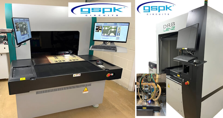
GSPK
|
Introducing our latest acquisitions: The CIMS Galaxy 25 Automatic Optical Inspection (AOI) Machine. This AOI system sets a new standard in precision, allowing us to inspect features down to 25um lines and spaces with unparalleled accuracy. Read more... Also a second Lenz DRB610 1+1 Drilling system, a testament to our dedication to excellence. We opted for another Lenz DRB610 1+1 due to its exceptional positional accuracy, heightened throughput, automatic drill checking, precision depth control using a second measuring system, and a substantial reduction in energy consumption. Read more... |
|
Jiva Materials |
Jiva and the University of Portsmouth have been awarded a Knowledge Transfer Partnership (KTP) by Innovate UK to further develop and commercialise Soluboard®, the world’s first biodegradable printed circuit board (PCB) laminate.
This collaboration aims to combat the increasing problem of electronic waste (e-waste) and offer a sustainable solution to the environmental challenges posed by the disposal of electronics. Read more... |
|
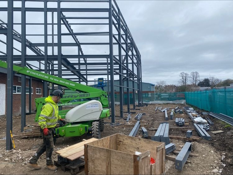
Newbury Electronics
|
Construction of our Faraday Road extension is now in its sixth week. Piling is complete and the steel frame was erected in just 1 week. A giant crane helps a bit. Read more... |
|
Strip Tinning |
Strip Tinning Automotive, a leading Electronic Component Manufacturer based in Birmingham, has big plans to grow the business in the next few years specifically in the automotive EV Battery and Roof Glass markets. Two years ago Strip Tinning Automotive decided to list on the AIM market, transforming into a PLC - a remarkable feat for a small-scale enterprise. This strategic move was primarily fuelled by their expansion into the EV battery market, specifically the supply of battery sensing components. They also recently raised £5m to support their EV division and specifically the development of its Cell Contacting System product for the EV battery market. Read more... |
| Go back to Contents |
| Section 10 |
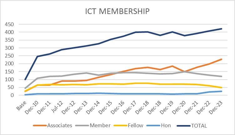
Membership News |
||||
 Bill Wilkie Bill WilkieTechnical Director and Membership Secretary, ICT. |
New Members
ICT Register of Members
ICT Membership Grading 2010 2023 |
||||
| Go back to Contents |

ICT Council Members |
|
|
Council Members |
Emma Hudson (Chair), Andy Cobley (Past Chairman), Steve Payne (Hon Deputy Chairman), Chris Wall (Treasurer), William Wilkie (Technical Director, Hon Sec, Membership & Events), Richard Wood-Roe (Journal Editor & Web Site), Jim Francey, Martin Goosey, Lynn Houghton, Pete Starkey, Francesca Stern and Bob Willis, |
Editors NotesThe ICT Journal |
|
|
Richard Wood-Roe |
Instructions / Hints for Contributors 1. As it is a digital format the length is not an issue. Short is better than none at all! 2. Article can be a paper or a text version of a seminar or company presentation. Please include data tables, graphs, or powerpoint slides. We can shrink them down to about quarter of a page. Obviously not just bullet points to speak from. 3. Photo's are welcome. 4. We would not need source cross references 5. Title of presentation Of course! Date, Job title of Author and Company represented. 6. An introductory summary of about 150 words would give the reader a flavour of what it's all about. 7. Style we don't want out and out advertising but we do recognise that the author has a specialism in the product or process that will include some trade promotion. Sometimes it will be a unique process or equipment so trade specific must be allowed. 8. Date and any info relating to where or if this article may have been published before. 9. We can accept virtually any format. Word, Powerpoint, publisher, PDF or Open Office equivalents. 10. Also, to make it easy, the author can provide a word file to go along with his original powerpoint presentation and I/we can merge it together and select the required images. 11. A photo of author or collaborators. I really do look forward to receiving articles for publication. Richard Wood-Roe |