“Yam awlroight, aer kid?” A friendly greeting in the local dialect as the Institute of Circuit Technology (ICT) held its 45th annual symposium June 4, 2019 in Dudley at the Black Country Museum—a symbol of the spirit of innovation in engineering technology and the entrepreneurial and manufacturing skills that had established that region’s supremacy in leading the original Industrial Revolution.
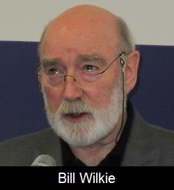
ICT Technical Director Bill Wilkie opened the proceedings with a good-humoured welcome address in which he likened delegates to kernels of knowledge and the ICT to a metaphorical watering can that encouraged their knowledge to germinate, flourish, blossom, and propagate.
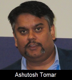
He was delighted to introduce keynote speaker Ashutosh Tomar, technical manager (research) with Jaguar Land Rover—the U.K.'s largest automobile manufacturer. Tomar’s speciality was the development of smart surfaces, structural and flexible electronics. His presentation entitled "Applications of Flexible and Hybrid Electronics in the Car" gave delegates the opportunity for a privileged look at some of the advanced electrical and electronic features hidden beneath the bodywork and interior trim of Jaguar Land Rover vehicles.
"Today’s automotive industry is as high-tech as aerospace. The electrical architecture is growing exponentially," said Tomar. He continued, "In our premium vehicles today, we have at least 175 features—probably double that if we include connected-car features and infotainment. The rate is continuing to increase with advances in self-learning, electric, and autonomous vehicles, which directly impact what goes underneath the body. And we have an ever-growing number of electronic control units in the car together with a rapidly increasing volume of sensors and smart sensors and their associated input-outputs and actuators inside of the car. There’s no room to put any more electronics!"
To illustrate some realities, Tomar’s graphics showed the locations of over 100 sensors, the enormity of a traditional wiring harness—eight kilometres of wire weighing 90 kilograms—and the complex labour-intensiveness of its construction. Tomar saw flexible circuits as the future of electrical distribution systems, and structural electronics as enablers for lightweight electronics features—such as displays, interior lighting, haptic sensing, and gesture recognition systems—building them into visible hard and soft surfaces within the car interior. He passed around an example of an integrated overhead lighting and control panel made by injection-moulded structural electronics technology, which offered a thickness reduction from 50 mm to 3.5 mm—a 60% weight saving and a 70% reduction in physical bill of materials.
Tomar went on to discuss possibilities in self-sustained wireless sensors—containing sensing, energy harvesting, battery technology, and transmission all in one package—and adapting flexible circuit and printed electronics capabilities to integrate electronic control units and electrical distribution systems. The effect would be to dramatically reduce mass and volume to eliminate large numbers of connections and achieve logistic benefits and a high level of automation in manufacture.
Although there remained some technical challenges to overcome and many thousands of hours of reliability testing to complete, it was only a matter of time before the full benefits of these concepts would be realised. It was clear that form was becoming at least as important of a consideration as a function: “What we can do is only limited by our imagination and vision!” Tomar’s keynote certainly captured the imagination of his audience and provided the basis of a very lively question-and-answer session.
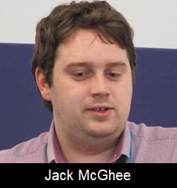
The closely related topic of printed electronics technology was the subject of the presentation by Jack McGhee who had recently completed a post-graduate study of new materials and methods at Loughborough University. Loughborough has a long history of formulation and characterisation of materials for printed electronics. McGhee explained that although the printing of conductive materials enabled inexpensive mass production of electronic devices that could be thin and flexible, those devices would typically have lower performance than conventional electronics. Whereas silver and carbon inks had most commonly been used, his research had examined the effects of integrating ceramic conducting and semiconducting materials into inks to improve their properties and increase their functionality. He discussed the incorporation of metal oxides, such as gallium-zinc oxide and indium-tin oxide, and more complex oxides, such as ferrites.
As printed, these materials gave some advantages over straightforward silver and carbon, but to achieve optimal conductivity, the materials required sintering and fusing. Of the several post-processing techniques investigated, some interesting results had been achieved with laser scanning, which could give effective local temperatures between 800°C and 1,300°C and decrease resistivities from typically 50 ohms per square to 3 ohms per square. Whereas originally it had been believed that simple fusing was the primary effect, McGhee demonstrated how the nanostructure of the materials could be manipulated by altering parameters and explored possible mechanisms. With indium-tin oxide, there was evidence that crystal growth occurred during re-oxidation, such that it formed microscopic wires and branched structures. And that the final structure depended on laser power and the optical properties of the material. He showed several examples.
Applications for laser-treated printed metal oxides included frequency selected surfaces, high-surface-area coatings for sensors, printed films for solar cells, tuneable capacitors, printed humidity sensors, and printed temperature sensors. There were also potential applications in 3D printed sensors. Ongoing printed electronics projects at Loughborough included screen-printed textile supercapacitors, printable active devices, and power dissipation through printed materials.
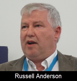
Extending the printed electronics theme to include stretchables, the final presentation of the morning session came from Russell Anderson, senior technical support specialist with DuPont Photovoltaic & Advanced Materials. “We know textiles, and we know electronics,” was a justifiable claim of DuPont with many years of history in those individual areas of expertise. And more recently, they had the opportunity to combine the two in wearable applications, for which a huge market was forecast and stretchability was a desirable attribute.
Anderson explained some of the science of wearable and stretchable performance, which required a balance between comfort and function, with reference to graphs of mechanical stress and electrical resistance versus strain. He also described a stretchable bi-layer thermoplastic polyurethane film composed of high-recovery and melt-adhesive layers supplied on a temperature-stable carrier. It was also designed so that a stretchable ink could be printed on the high-recovery surface and the melt-adhesive layer used to hot-press bond it to the fabric. A silver-loaded screen-printing ink had been developed with the metal in the form of fine flakes suspended in a thermoplastic elastomer resin. During the drying step, the solvent was removed, and the conductive particles packed together forming electrical pathways. He showed the results of 100% stretch testing and 80-cycle 10% strain testing—both of which maintained low electrical resistance—and functional wash testing based on 50 cycles of the ISO 6330 colour fastness test with minimal increase in resistance.
A typical volume production sequence for the incorporation of conductors into apparel was to screen-print circuits onto the polyurethane substrate, singulate the patterns by die-cutting or laser-cutting, hot-press-bond the circuits onto fabric, add any functional components, and then assemble the garments. Applications included sportswear for monitoring respiration and heart rate, heated industrial winter wear, and various medical monitoring functions and automotive heaters and sensors.
Dodging the showers, delegates made their way down the hill to the authentic reconstruction of a 1930s High Street and queued up to enjoy a traditional lunch at Hobbs and Sons Fish and Chip Shop. Some paused to admire the Sunbeams at Hartill’s motorcycle shop and had to hurry back uphill to return to the conference room and the 21st century for the afternoon session.
"High performance automotive and power electronics begin with innovative materials," was the opening line of an enlightening discussion of insulated metal substrates and thermal interface materials from Robert Art, global account manager IMS/TIM for Ventec International Group. He listed the basic components of a typical IMS material—a metal base layer, a dielectric layer, and a circuit layer. Then, he looked more deeply into the realities of their properties and how they needed to be considered from a different perspective than those normally associated with FR-4 laminates when specifying materials for particular applications.
Beginning with glass transition temperature (Tg), for the gradual and reversible transition in amorphous materials from a hard and relatively brittle state into a rubbery state with increasing temperature, the popular perception was that this should be very high. This was true for achieving mechanical stability in regular FR-4 multilayers, but in IMS materials, a lower Tg was preferable. This enables the dielectric to act as a compliant interlayer between components with expansion coefficient typically 10 ppm/°C and the aluminium baseplate with expansion coefficient typically 23 ppm/°C, hence reducing any tendency to cracking of solder joints under thermal cycling.
Clearly, the primary reason for using IMS substrates was to conduct heat away—“LEDs get destroyed not because of current but because of heat”—but there was still some confusion in terminology (e.g., thermal resistance, thermal impedance, thermal conductivity, etc.) and different test methods could give widely different results. It was important that the customer carried out their own tests before specifying a particular material rather than relying on nominal data-sheet values.
Voltage-withstand testing depended on the application and was linked to the operating voltage of the system. UL required the test voltage to be twice the operating voltage plus 1,000, and users typically asked for higher values than that. Art emphasised that each test stressed the material, and the circuit should still work after testing rather than be tested to destruction.
He went on to discuss Ventec’s range of IMS materials, and the technology roadmap showing the typical applications for which they had been developed. In applications where solder-joint cracking was a critical reliability issue, the newer materials had dielectrics designed for elastic deformation and low-expansion aluminium alloys to minimise mechanical stressing.
Art examined a series of alternative design concepts for thermal management with IMS substrates and special surface treatments and demonstrated applications and benefits of electrically conductive and insulating thermal interface materials. He emphasised the importance of choosing the right material from a cost-performance standpoint but added a note of caution in advising OEM designers to avoid nominating too many different materials and causing inventory and stock-control problems for the PCB fabricator.
Taking the guesswork out of copper distribution in pattern plating operations was the subject of the final presentation by Robrecht Belis, manager of the Surface Finishing Business Unit at Elsyca in Belgium.
Achieving relatively uniform deposit thicknesses across complicated panel designs was a task that had historically relied heavily on the combined experience of pre-production and process engineers and had inevitably involved a lot of trial-and-error and compromise. Belis described graphical simulation software that could be straightforwardly configured to a specific plating geometry and electrolyte, panel size and pattern, and process parameters based on a virtual mockup of the real-life plating tank and flight bar. Alternative panel configurations and the effects of shields and robbers could be quickly evaluated. The software enabled a substantial improvement in plating uniformity and provided detailed information on copper thickness distribution and potential quality issues.
ICT deputy chairman Steve Payne, managing director of Cirflex Technology Ltd, brought the symposium to a close, thanking speakers for sharing their knowledge and the quality of their presentations, delegates for their attention and support, and particularly Bill Wilkie for organising an exceptionally interesting and relevant programme.