
Institute of Circuit Technology
38th Annual Symposium.
Duxford, UK, 12th June 2012
Renowned for his ability to locate impressive venues for Institute of Circuit Technology events, ICT Technical Director Bill Wilkie made yet another excellent choice and brought the UK printed circuit industry together at the Imperial War Museum in Duxford near Cambridge for the Institute's 38th Annual Symposium, on the theme of Manufacture and Materials.
 ICT Vice-Chairman Dr Andy Cobley opened the symposium, welcomed the many delegates and introduced keynote speaker Bill Burr, who captured the attention of the audience with his views on inspirational intuition, with particular reference to the development of PCB technology from Paul Eisler to the present day and beyond: "Knowledge plus perseverance plus intuition equals the anatomy of a brainstorm, and intuition is one of the most brilliant aspects of the higher unconscious"
"People who lived the problem developed and invented solutions", he continued: "Inspiration is the fruit of perception and perspiration."
Taking microvia technology as an example of an innovation that enabled a whole new generation of electronics, Burr made it clear that it was PCB manufacturers who developed the technology – "you couldn't buy it in a bucket!" and invariably the PCB manufacturer occupied the position of translator – standing between the material supplier and the subsystem manufacturer, understanding the languages of both sides and turning materials into electronic function - effectively translating smart molecules into smart products.
Moving back to the future, Burr discussed added value and how western-world PCB manufacturers could retain value by providing enabling technology in order to regain the high ground, break away from the commodity trap and make a difference by studying industry trends, new and emerging applications, product characteristics, global issues, component packaging trends and customer roadmaps. Against this backdrop, he described a project in which he was cooperating with Nick Pearne of BPA called Metal-in-the-Board, MiB. Increasing power density in electronic devices in general, and the rapidly increasing utilisation of electronic control of electrical power opened up a new generation of opportunity for innovation in thermal management, particularly in automotive and electro-mobility applications.
In a Quo Vadis sum-up, Burr urged delegates to stay alert for opportunity, to watch and guard the added value, and to sell the advantage, not the commodity.
 Next to present was Bob MacRae from Taiyo America, who explored all the options, advantages and disadvantages of via-hole plugging techniques. Typical reasons for plugging vias were to prevent corrosion of the via connection, to improve vacuum performance at in-circuit test, to prevent solder wicking into via holes connected to SMT pads, to prevent contamination under components, to gain back outer layer real eatate and, in sequential builds, to fill buried vias without voids and reduce prepreg loss. Three decades ago, it had become common practice to tent via holes with dry-film solder mask and since the introduction of liquid photoimageable solder masks there had been many permutations of procedure for achieving the equivalent with liquid materials. In most cases, removal of solvent was a major issue hindering the success of these techniques and, unless a 2-stage final cure or a vacuum chamber were used, popping or outgassing could occur during soldering. Incomplete hole plugging could lead to chemical entrapment and result in field failure as well as skip plating of ENIG.
High-performance hole-filling pastes were now available which offered the best combination of performance and reliability. These were based on zero-solvent formulations which showed little or no shrinkage on curing, giving flat, planar plugs which could be plated-over. Moreover, these materials were compatible with high-performance laminates in terms of glass transition temperature and thermal expansion characteristics.
 Standing-in on behalf of Professor Martin Goosey, Pete Starkey gave an update on the EU FP7 projects ASPIS and Susonence. ASPIS, a 3-year project to enhance the performance of nickel-gold solderable finishes, had the key objectives of
investigating the fundamental failure modes and mechanisms of ENIG coatings, developing an ENIG screening tool, developing improved coating methods and materials based on aqueous and ionic liquid systems, and verifying the compatibility of technology developments with established assembly methods and practices.
The project had reached a half-way stage and already a clearer understanding of the underlying chemistry, physics and metallurgy of the ENIG process was emerging. Some encouraging progress had been made in the study of alternative chemistries, and an initial examination had been made of non-destructive predictive test methods. The ICT continued to disseminate up-to-date information through presentations, technical papers and press releases, and the ASPIS website www.aspis-pcb.org was proving to be an effective resource.
Susonence - Sustainable Ultrasonically Enhanced Chemical Processes, was a multi-partner project developing advanced sonochemical processes to reduce chemical usage and decrease waste in the PCB and metal finishing industries, with the key aims of implementing ultrasonically enhanced surface modification processes for removing surface layers, etching, and texturing a variety of widely used substrates with greatly decreased chemical consumption, enabling a step-change in competitiveness within the surface finishing and printed circuit board manufacturing sectors and significantly decreasing environmental impact. Expected benefits were reduced use of toxic and hazardous chemicals, waste minimisation and diversion from landfill, reduced energy consumption and reduced water consumption. Up-to-date project information could be found on the Susonence website
Markus Kurz from Panasonic gave an overview of material innovations with a focus on power electronics. Objectives were to achieve high soldering reliability for PCBs with thick copper, long-term insulation reliability both within the structure of the board and upon its surface, and heat dissipation solutions.
Regarding insulation reliability within the board, Kurz discussed the factors influencing the formation of conductive anodic filaments, CAF. These were apportioned approximately 50/50 between PCB manufacturing process conditions, particularly those related to pressing, drilling and plating, and laminate properties such as the completeness of impregnation of glass fibres by resin, adhesion of resin to glass, ionic impurities and the heat resistance of the resin. He showed some actual examples of CAF failures, both in the laboratory and in the field. In Germany, ZVEI were working on a method for CAF evaluation appropriate to automotive applications, with test conditions 85% RH, 85ºC, 100v and an insulation resistance requirement greater than 10 MΩ. Insulation resistance on the surface of the laminate was measured by its comparative tracking index CTI and classified according to EN 50124 or UL. Halogen-free materials had been shown to give higher CTI values than standard FR4.
Power electronics demanded effective thermal management, and thermally conductive laminates could free-up real-estate on PCBs by reducing the requirement for thermal via holes. Whereas standard FR4 had a thermal conductivity around 0.4 W/mK, certain filled laminates could now achieve values as high as 4W/mK.
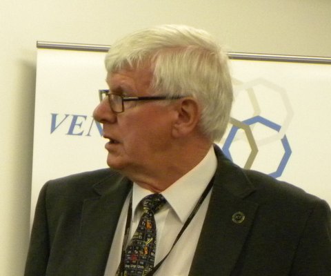
 Bill Wilkie moderated the afternoon session and introduced as his first speaker Lawson Lightfoot, who described the details of the recently-launched Rainbow fine-line imaging process. Key to the technology was a liquid etch resist with very high photospeed, developed with the cooperation of Electra Polymers. A unique feature of the resist was that it could be exposed immediately after coating and without drying. A proprietary coating on the photomasters prevented them sticking to the resist, and the very short optical path enabled the imaging of lines and spaces as fine as 20 microns without the need for collimated light: LED arrays were used as the UV source.
The compete Rainbow automated process line was compact, occupying only 12 square metres of floor area including its own clean-air enclosure, and had very low power consumption, about 3 kW. It was designed to deliver a double-sided panel, ready for etching, every 15 to 20 seconds and a full system would be made available for customer evaluation during Q3 2012.
 "Printing, coating and nano-imprinting equipment and processes for large area printed electronics", was the topic of the presentation of Thomas Kolbusch, Vice President of Coatema Coating Machinery and member of the board of the Organic Electronics Association. Coatema had over 30 years' experience in the production of coating and printing equipment with a background in the textile industry, and had established a major R&D centre in Germany. Kolbusch gave a comprehensive overview of the available printing and coating systems that could be applied to the manufacture of printed electronics from small batch-type coaters to large roll-to-roll systems.
He reviewed market projections for organic and printed electronics with reference to the OE-A roadmap, listing organic photovoltaics, flexible displays, OLED lighting, electronics & components and integrated smart systems as principal areas of development, then discussed the range of different existing and not-yet-existing roll-to-roll production technologies and processes requiring to be integrated to enable successful printed electronics manufacture, taking the in-line fabrication of organic photovoltaics as an example. Key technology hurdles were resolution, registration accuracy, layer thickness, pattern on pattern precision, environmental control and inline quality management. A wide choice of printing and coating techniques could be used to suit various applications, and Kolbusch made specific reference to slot-die coating as a technique with great potential in printed electronics.
Many organisations were engaged in research, and an FP7 project, FACESS – Flexible Autonomous Cost Efficient Energy Source and Storage – had recently been completed, demonstrating the manufacture of efficient organic solar cells and thin film batteries on flexible substrates using commercially available materials and cost efficient roll-to-roll mass production techniques.
Looking to the future, Kolbusch was under no illusion that many challenges lay ahead, funding for industrial up-scaling was required and the industry needed to define processes and standards. The European industry was largely composed of SMEs and he believed that this was where its strength lay, provided the SMEs took a joined-cluster approach to driving the technology forward with the support of global networks like the Organic Electronics Association and the Large-area Organic Printed Electronics Convention.
 The final presentation came from Mark Knowlton of KPS, business improvement specialist and advocate of lean manufacturing, and was entitled "Lean and Benchmarking – a driver for growth". He described how a lean methodology could be applied to drive cost out of the business and achieve increased capacity, improved price competitiveness and reduced lead times, with streamlined and efficient business processes that were fit for purpose. The process began by establishing what it was that customers really valued, then mapping the value stream and eliminating non-value-adding activity to create more capacity for value adding activity and growth. The five golden rules were: to speed-up the order fulfillment cycle, to make only what could be sold, to buy only what was needed, to reduce work-in-progress and to collect what was owed. And the two main pillars of lean were continuous improvement and respect for people. Knowlton listed lean principles, tools and techniques, the eight wastes and the eight key competences, and illustrated the differences between supplier and customer perspectives and perceptions with regard to the supply chain. He emphasised the importance of benchmarking as a systematic process for identifying and implementing best practice and learning from the experiences of others, quoting the Cheshire Cat from Lewis Carroll's Alice in Wonderland: "If you don't know where you are going, any road will lead you there"
Bill Wilkie wrapped up the symposium, thanking speakers and delegates, acknowledging the generous support of Lamar Group and reporting that ICT educational courses were remarkably well subscribed and that the Institute continued to gain membership.
As the audience dispersed, very few went straight home – the opportunity to see some of the attractions of the Imperial War Museum was too good to miss! The only disappointment was that we were not allowed to take photographs...
Pete Starkey
June 2012