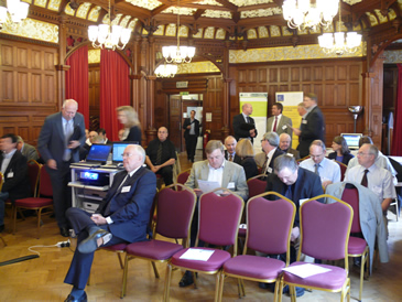
ICT Annual Symposium June 2009
Bletchley Park, in Buckinghamshire UK, is the former stately home taken over by the British Government shortly before World War Two to be the secret base of the Government Code and Cypher School, which broke the reputedly unbreakable Enigma code and enabled British Intelligence to make sense of enemy communications: a historic and distinguished venue for the 35th Annual Symposium of the Institute of Circuit Technology.
Opening the Symposium, themed “Printed Electronics”, ICT Technical Director Bill Wilkie welcomed faces old and new and reflected upon the continuing success of the Institute, and its steadily growing membership.


Dave Wayness of Dow Electronic Materials focused on inkjet from a material supplier’s perspective with a presentation entitled The Use of Inkjet Printing Technology for Fabricating Electronic Circuits, sub-titled The Promise and The Practical. The promise included elimination of photomasks, faster job turns, off-contact imaging for delicate substrates, image compensation and registration, higher yields and reduction in materials wastage. When it came to practical reality, inkjet fabrication of electronic devices was still very early in its maturing process and, echoing the comments of Steve Jones, although 300 dpi resolution was satisfactory for graphic arts it was far from adequate for electronics, which would require resolution of 750 to 5000 dpi for features to be continuous, uniform and functional. He discussed in detail the ways in which high-resolution images could be generated by multiple-pass and interlacing, taking as example a 75 micron line and space conductor geometry at 1250 dpi. Using an array of 15 heads, a 24” x 18” panel could be printed in 24 seconds. Dow had designed a hybrid UV phase-change etch-resist ink, for use with heated print-heads – liquid at jetting temperature but solid at room temperature so that flow-out was minimal once it hit the substrate surface – which gave excellent image definition. There had been significant increase of interest in solder mask imaging, particularly on designs with solder-mask-defined pads where image placement accuracy was critical, and Dow’s method of photo-tool elimination by inkjetting a UV-opaque negative image on to standard liquid photoimageable solder mask obviated all of the concerns regarding product qualification which had hindered the adoption of direct inkjet solder mask formulations.
Professor David Harrison’s Cleaner Electronics Research Group had been working for many years at Brunel University on methods for producing circuit interconnects and passive components on various flexible substrates using offset lithography, a faster and higher resolution technique than screen printing. More recently, research had been directed at methods for producing voltaic cells by similar techniques, so that printed electronics devices could be powered by batteries produced in-situ. Leclanché cell chemistry, using zinc and manganese oxide with an ammonium chloride electrolyte, had been chosen as the basis of a feasibility study, and inks with properties suitable for offset litho printing had been developed to prove the concept. Changing from a zinc-particle to a zinc-flake system had improved performance, as had the use of a carbon intermediate layer and silver current-collectors. Batteries had been produced with capacities of 10 milliamp-hours, capable of delivering a peak current greater than 150 milliamps, although shelf-life remained a major limitation, 10 days being typical, and this was being addressed in ongoing work. Professor Harrison demonstrated as a working example a musical greetings card where both the interconnect and the battery had been produced by offset litho printing.
Frank Eirmbter of SunTronic Electronic Materials presented a broad survey of inks and chemicals for printed electronics. He explained the principles of various printing techniques – letterpress, gravure, flexo, pad, screen, offset and inkjet, and how the different processes required inks with different characteristics. The only printing process traditionally associated with printed circuit manufacture was flat-bed screen printing, although rotary screen, rotogravure and flexography were now being applied to the production of hybrid devices and RFID tags. Offset lithography and inkjet printing were emerging as techniques for printed electronics. SunTronic were able to offer inks for all of these processes, and he listed many applications including antennae, membrane switches, capacitors, shielding , sensors, photovoltaics, RFID, displays, automotive, telecom, medical and diagnostic. Taking a membrane switch as an example, he described the manufacturing process and the specific products: graphics inks, silver conductive inks and flexible UV dielectric inks, used in fabricating the intermediate components. A second example he demonstrated was the construction of an RFID “smart label”. RFID antennae could be printed directly onto cardboard boxes using a flexo-printed water-based silver ink. Other applications illustrated included flexible displays, printed resistors, transducers and sensors, and development would continue on functional inks for a whole range of new applications.

The Lunaris system was a drop-in replacement for traditional photolithographic and laser-direct-imaging processes, taking the work direct from base laminate to etch-resist image in a single step. Océ’s extensive knowledge of drop flight and drop flow characteristics had indicated that a hot melt ink was most suitable for this application, and they had engineered a specific formulation compatible with their own design of heated print-head. The Lunaris machine incorporated 60 print heads, each of 260 nozzles capable of firing at 10 – 20 MHz. Although Océ’s heads were claimed to be the most reliable in the world, statistically a failure rate of 1 in 1 billion droplets was expected, due to air entrapment in a print channel. A unique feature of Lunaris was the ability to predict such failure, and in operation only 1 in 3 print heads was in use at any instant, the system switching to an alternative row of heads every 20 seconds, with an additional row of heads always available as a standby, so that the one-in-a-billion failure was eliminated and a perfect image was guaranteed. The machine had a production capacity of 60 double-sided panels per hour, and was attracting keen interest in the market.

Pete Starkey
ICT Council
June 2007
