ICT 36th Annual Symposium, "New and Emerging Technologies"
15 June 2010
The 36th Annual Symposium of the Institute of Circuit Technology was held on 15th June 2010 at the National Motorcycle Museum near Birmingham, England.
 ICT Chairman, Professor Martin Goosey, welcomed a full house of delegates and was pleased to report that the Institute’s membership numbers continued to increase and that the ICT had been appointed project coordinator of the European Framework 7 ASPIS project on solderable finishes, which was currently at the contract negotiation stage. As a prelude to the symposium programme, Professor Goosey briefly reviewed some emerging technologies and their implications for circuitry and interconnect. Interconnection was driven by device technology, and semiconductors, already at the 32-nanometre node, were expected move towards the 22-nanometre node during 2011-2012. Intel had already developed a 64Gb multilevel cell NAND flash device at 25 nanometres that represented a data-per-unit-area utilisation of 0.00138 square microns per bit. Could the trend continue? It was clear that the PCB and interconnection industry would continue to face challenges to provide interconnects for increasingly complex devices and their packages, and that the PCB would increasingly become integrated a functional component of electronic devices. Professor Goosey introduced a programme of six presentations, all topical and relevant to the “new and emerging technologies” symposium theme.
 First two presentations each focused on photovoltaic technologies, and Tony Ridler from Dow Chemical began his photovoltaics overview by quoting a forecast that the world annual electricity demand would likely double by 2030 to 3 terawatt hours. Solar energy presently represented only 0.3% of world electricity generation capacity but hypothetically had the potential to fulfil the global demand more than 8000 times over. With reference to the social, political, environmental and economic drivers for photovoltaic power generation, he observed that cost per watt peak was the overriding issue, and examined the various existing technologies for the manufacture of solar cells. Two principal technologies were evident: crystalline silicon and thin film. Thin film was rapidly evolving, particularly in China, India and Taiwan, and was typically based on glass with vapour-deposited copper-indium diselenide, each panel becoming in effect a single solar cell. But whilst research continued on different thin-film approaches, the world photovoltaics market remained dominated by crystalline silicon wafer-based technology, even though costs of materials, specifically silicon and silver, were significantly higher than for thin film. A typical 80-metre production line had a annual capacity of 15 million wafers, equivalent to 45 megawatts. Ongoing development objectives were to increase the conversion efficiencies of solar cells in terms of watts per unit area, whilst reducing material costs per watt and improving manufacturing yields.
 Tony Ridler’s paper neatly prefaced the presentation of Frando van der Pas from Enthone in the Netherlands, who indicated that the immediate goal of the photovoltaic market was to achieve “grid parity”, the point at which the cost of a kilowatt-hour of solar energy equated to that of electricity generated from other fuel sources, and it was anticipated that this might be achievable within the next few years. He explored routes to cost reduction in solar cell production, with the initial target of reducing cost per Watt to less than one US dollar, then working down towards a cost of $0.65. There had been a substantial increase in the production of solar-grade silicon, which was a major cost factor, and wafers were being sliced thinner. New manufacturing methods were being introduced to achieve higher efficiencies per cell and to further reduce material costs. One of these was to increase the available top-side area by reducing the line-width of silver contact patterns, with the added benefit of substantial savings in metal cost. The established technique for forming these contacts was by screen-printing silver paste. The new methodology used electroplating, initially on a fine-line screen-printed silver base layer, but with the ultimate objectives of eliminating screen-printing using direct metallisation, and subsequently eliminating the use of precious metals. Because photovoltaic manufacture had evolved out of the semiconductor industry and depended largely on batch-production techniques, there was scope for a change of production philosophy towards a more cost-effective PCB-type approach. Continuous electroplating equipment already established in PCB fabrication could be adapted for processing solar cells, and the mainstream electronics industry was beginning to recognize the opportunities presented in photovoltaic manufacture. Working partnerships had already been announced between AT&S and Solland Solar, and between Schweizer and SMA Solar Technology
 Mark Goodwin, MD of Ventec Europe, spoke on the topic of Thermally Conductive PCB Substrates in a context of the increasing need for dissipation of heat from electronic modules, with particular reference to the dramatic growth in applications of high-brightness LEDs. Reviewing available methods for heat transfer and dispersal, he explained that insulated metal substrates had become established as preferred base material for the manufacture of circuits for LED applications, and offered cost effective performance with straightforward fabrication, good mechanical stability and a range of thermal conductivities to suit particular configurations. These materials typically consisted of copper foil bonded to an aluminium substrate with a thermally conductive FR4-type bonding resin, either woven-glass reinforced or non-reinforced, heavily loaded with ceramic filler. The choice of dielectric for a given application was determined by the need to achieve a balance between thermal conductivity, dielectric strength, reliability and price. In general, reinforced dielectrics had lower thermal conductivity, but higher breakdown voltage, superior thickness uniformity, and cost less than non-reinforced grades. Woven glass reinforcement of the dielectric reduced its coefficient of thermal expansion both in the XY plane and in the Z-axis, such that the CTE mismatch between copper, dielectric and aluminium was significantly less than for unreinforced dielectric, a significant factor in determining reliability. Goodwin urged designers to think in terms of the actual thermal impedance of an insulated metal substrate, rather than its Watts per metre Kelvin coefficient, and to avoid taking data sheet values too literally without performing their own qualification tests to select materials to suit specific applications.
 Dr Andy Cobley described a research programme being carried out at Coventry University to investigate the feasibility of using ultrasonically dispersed copper nanoparticles for plating through-holes in printed circuits. Two routes had been considered: using the nanoparticles as a palladium replacement for electroless copper initiation, or as a direct metallisation process to form a conductive layer for subsequent electroplating. A characteristic of nanoparticles was their tendency to agglomerate, and ultrasonics was a more reliable method than mechanical agitation for keeping them dispersed. Experiments to functionalise through-holes using 50nm copper nanoparticles, ultrasonically agitated at 40KHz, as initiator for electroless copper had shown some encouraging results, although coverage so far observed was inferior to that achieved using palladium initiation. Work was continuing to investigate the effects of frequency, intensity and conditioner chemistry. Direct plating trials had not been successful: even at increased nanoparticle concentration, electroplate penetration into the holes was minimal.
 Francesca Stern of BPA steered the subject from technology to market research, using her “driving a car” analogy to illustrate the dependence of management on good forecast information to support the decision-making process, as she presented an analysis of worldwide market and technology trends in the PCB industry. European multilayer PCB prices were generally trending upwards, although there remained a substantial price differential between Europe and Asia. Production was growing back towards 2008 levels in China, Korea and Taiwan, and Asia’s market share was increasing at the expense of Europe and North America. World PCB production had grown from 42 billion USD in 2000 to 49 billion USD in 2008 and during that period North America’s share had fallen from 27% to 9%, and Western Europe from 12% to 7%, whilst China had grown from 8% to 29%. The UK’s share of the European market had fallen from 17% of 5.2 billion USD in 2000 to 9% of 2.3 billion USD in 2009, and it was interesting to note that of 51companies manufacturing PCBs in the UK, only 5 were turning over more than 10 million USD, 7 between 5-10 million USD and 21 between 1-5 million USD, whereas Germany had 78 in total, of which 22 were turning over more than 10 million USD.
 Back to technology for the final presentation, Dr David Selviah of the Department of Electronic and Electrical Engineering at University College London, gave an overview on the 3-year Integrated Optical and Electronic Interconnect PCB Manufacturing OPCB project, which had been supported by EPSRC, the UK Engineering and Physical Sciences Research Council, via IeMRC, the Innovative electronics Manufacturing Research Centre. Dr Selviah commented that at data rates in excess of 10 Gb/sec, copper interconnect would become more seriously affected by the fundamental constraints of high frequency electronic data transmission such as dielectric loss, skin effect, crosstalk and electro-magnetic interference. As 12 Gb/s is now on the roadmap for data storage system manufacturers there was considerable interest in incorporating optical waveguides into PCB backplanes for communication between central processor arrays, hard disk drive arrays and through data routing switches. Benefits of optical interconnection included low loss, low cost, low power, low crosstalk and low clock skew, but they were unable to transmit electrical power. The OPCB project explored methods for manufacturing optical waveguides within a polymer layer incorporated into the structure of PCB backplanes, with in-plane butt connections to VCSEL transmitters and detectors, using techniques compatible with those already established in commercial PCB manufacture. Several processes and materials had been evaluated for waveguide fabrication, including direct laser-writing with a Helium-Cadmium laser on photo-polymerisable acrylic resin, laser ablation using Excimer, Nd-YAG and CO2 lasers on acrylic or polysiloxane resins, inkjetting with UV-curable polymer, and photolithography. Methods had been developed for characterisation of waveguide performance, by modelling and by measurement, to enable design rules to be formulated for incorporation into PCB CAD systems. Dr Selviah showed examples of system-demonstrator assemblies, and quoted performance data for crosstalk, optical loss and misalignment tolerance.

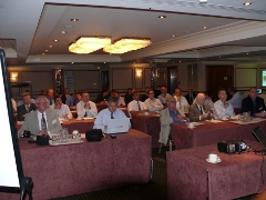 The Institute of Circuit Technology continues to thrive. This was an outstanding Annual Symposium: an informative and well-balanced programme, first-rate presenters, an attentive audience and a superb networking opportunity. The venue was well chosen: central location, excellent conference facilities, and ICT Technical Director Bill Wilkie had negotiated free admittance to the museum for delegates. There seems to be a remarkable synergy between motorcycling and PCB manufacture – maybe the noise, the smell, the element of risk, the feeling of being not quite in control – and it’s amazing how many PCB guys are past, present or aspiring bikers.
 Francesca Stern receives her Certificate of Fellowship of the ICT
 Dr Andy Cobley receives his certificate of Fellowship of the ICT
 Professor Goosey among the Nortons
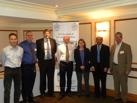 Speakers
