| ICT Annual Symposium Review June 6th 2023 | |
 Bill Wilkie Bill Wilkie |
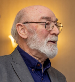
After a long crawl through heavy traffic on the M42 motorway, it was a great relief to exit at Junction 6 and arrive at the National Conference Centre for the 2023 Annual Symposium of the Institute of Circuit Technology on June 6. The conference centre is co-located with the historic National Motorcycle Museum and situated in the heart of the UK midlands, a stone’s throw from Birmingham International Airport. The delegates were welcomed by technical director Bill Wilkie. With reference to his grandson’s 5-a-side football team being instructed to “get into shape,” he commented on the changing shape of the UK PCB industry and how the Institute would continue to adapt to its geographical distribution in the choice of symposium and seminar venues. Interesting to see where we might be travelling to next year. |
|
|
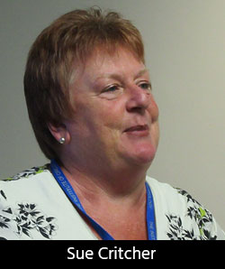
The keynote presentation came from Sue and Andy Critcher, partners in a design consultancy called Total Board Solutions, with a review of the latest design requirements for board fabricators. Sue Critcher reflected upon developments in PCB design from the days of her apprenticeship, where she was hand-taping tracks and pads in the drawing office, to now using the latest design, simulation, and analysis tools, often with mixed analogue, digital, and RF technology on a single PCB. Besides the challenges of shrinking component dimensions, signal integrity, and power integrity considerations, and the increasing requirement for thermal management, project timescales are getting shorter, and the pressure is always to deliver the design more quickly at less cost. Andy Critcher reviewed some of the implications of mixed signal designs and the importance of correctly defining the stackup, particularly with the increasing complexity of RF structures. Documentation is a major concern. What data format to use: RS-274X or ODB++? RS-274X2, or even IPC-2581? He commented that not all versions of ODB++ are the same. Fabrication drawing data was another minefield, especially where the template was “copied from the last job.” Another danger area was specifications when the designer was not necessarily aware of the implications. As designers, the Critchers displayed a remarkable awareness of the challenges faced by the PCB fabricator—a consequence of spending time over many years visiting, discussing, and collaborating. Common issues with data sent from designers included drawings and specifications, annular rings too small, minimum copper spacing, clearance to pad, copper distribution and copper balancing, etch compensation, teardrops, mouse and rat bites, slivers, as well as all sorts of solder mask and silk screen issues. |
|
|
Andy Critcher spent some time discussing CAD-CAM checks, remarking, “We are checking the same thing, right?” He commented that several of the major CAD systems offer DFM capability, but remarked that although many CAD systems are available—he listed 24—each system is different. What did the future hold? As a representative of the “old guard” who had started on the drawing board and come through the ranks, learning their craft from others along the way, Sue Critcher is concerned about the current status of the PCB design industry. The world of PCB design is changing. The average age increases by a year every year and the “old guard” is moving on. A recent survey indicated that 61% of designers are aged 50 plus, only 23% are younger than 35, and 55% of designers plan to leave the profession within the next 10 years, with more than 25% retiring within five years. The “new blood” is electronics engineers from university. CAD systems continue to improve but can only take them so far. Where will these engineers get their layout knowledge and learn good practices as PCB complexity increases? The parting advice from Sue and Andy: “Talk to your fabricators!” |
|
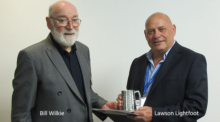
Following the Total Board Solutions keynote, Bill Wilkie took the opportunity to award certificates to new corporate and individual members, and to make a special award to Lawson Lightfoot upon his retirement from the ICT Council. Bill acknowledged the enormous contribution that Lawson had made over many years, particularly in the area of technical training and the sharing of the educational resources of the Northern UK Circuit Group. He was appointed an Honorary Fellow of the Institute.
|
|
|
|
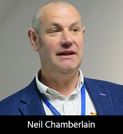
“Impedance and Beyond” was the title of the presentation of Neil Chamberlain from Polar Instruments. Referring back to “a few years ago” when he did a major house refurbishment, he learned two things: It’s important to have the right tool for the job, and to know what you’re doing with that tool. (He admitted that during his house refurbishment he had neither.) But acknowledging that within the seminar audience he was addressing designers, laminate manufacturers, and PCB fabricators, he described how Polar has always endeavoured to provide the right tools for the job and to give fabricators a coherent suite of tools for modelling impedance with a field solver, designing and documenting stackups, generating meaningful test coupons, and measuring them. “Who should design the stackup?” was a commonly asked question, whether it should be the OEM, the design guy, or the fabricator. The answer: “It depends on the customer, the requirements of the board, and the complexity of the design.” Polar has built a library of materials that covers the range that the laminators have developed over many years to fill the spectrum between standard FR-4 and Rogers 4350. It is inevitable that when a designer specifies a higher-grade, higher-performance material, someone will put a multiplier on the cost of the board. The designer must justify that cost. The library of materials allows simulations to be made with various laminates in various environments, to work out whether the material is actually required, whether standard FR-4 will give an acceptable performance, or whether the attributes of the higher-specification material are essential. All of this is specific to an individual design. Additionally, the stackup tool can generate a test coupon to enable critical parameters to be physically measured. “What loss can I expect on my system?” was another commonly asked question. “What frequency can I run this transmission line at and still get the signal I want at the other end?” Chamberlain likened a transmission line to a coaxial cable. Whatever the characteristic impedance, the longer the cable the greater the loss. Characteristic impedance is only concerned with the cross-section, not the length. However, another solver was available that could predict the losses expected along the line at a particular frequency depending on material, copper geometry, and copper roughness. Designers need to know that these methods exist and that a broad range of materials are available to avoid “taking the easy way out” and incurring the costs of over-specification. Chamberlain reviewed parameters affecting loss, discussing copper roughness and the skin effect in detail, and emphasising that at frequencies above 1 GHz the roughness of the copper could be a more important factor than the laminate itself. Therefore it was increasingly important to understand effect of the positions of “smooth” surfaces and “rough” surfaces within the stackup, and the benefits or otherwise of reverse-treated and low-profile foils. With lunch-time looming, Chamberlain’s presentation provoked much interactive discussion, involving designers, laminators, and fabricators. It was such an interesting interlude that delegates were more inclined to listen and participate than to rush off to get fed. Lunch was slightly delayed, but everyone made it back for a prompt start to the afternoon session. |
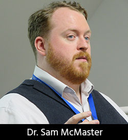 |
Dr. Sam McMaster from Pillarhouse International discussed some of the challenges encountered in selective soldering and described how training needs are being met. Reviewing the primary elements of selective soldering, he considered options for fluxing, preheating, and soldering techniques. The drop-jet method gives very accurate flux application with minimal flux consumption and reduces the need for PCB cleaning. It can be used with water-based or alcohol-based fluxes and requires little maintenance. He demonstrated a system in action with a video clip. By comparison, ultrasonic fluxing offers rapid flux application with a high solids capability. Like drop-jet, it can be used with water-based or alcohol-based fluxes and requires minimal maintenance. Pre-heating can be done by infra-red or convection and carried out before, during, and/or after fluxing, depending on the thickness and thermal mass of the assembly and the residual activity of the flux. His video illustration showed top and bottom-side temperature monitoring. McMaster talked in detail about soldering parameters. He advocated for nitrogen inertion to maintain good flow characteristics and reduce the amount of bridging and dross generation, with 50 ppm of oxygen as an upper limit. The solder bath is positioned to apply solder to the underside of the PCB, either to a single joint by a dip step or programmed to move along rows of connectors as a series of draw steps. Longer contact times can aid wetting and pull-through of solder but can also dissolve copper from the PCB. The composition of the solder alloy determines its liquid properties and the subsequent mechanical properties of the solidified joint. Non-wetting dip nozzles can be used for fast production of high-volume products, but they lose the “per-joint” customisation facility of a wetting nozzle. Solder temperature was chosen to balance good pull-through vs. flux activation loss and the increased likelihood of oxidation. It is typically in the range of 280–320°C. Top-side heating during soldering can be used if the assembly has a high thermal mass that requires continuous heating to ensure good solder pull-through. Pillarhouse typically holds the PCB stationary during soldering, whilst moving the soldering bath and nozzle. The use of a laser positioning sensor allows live offsets to the programmed height to compensate for board warpage and achieve good soldering. Their Selective Soldering Academy provides real-world selective soldering training in troubleshooting and defect identification to IPC standards, defect examination, and elimination by control of process parameters, understanding differences in leaded and lead-free solders and surface finishes, design for manufacture with selective soldering in mind, and gaining a better understanding of machine features and their applications. |
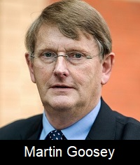 |
Although LED lamps may have a quoted life expectancy of 20,000 to 50,000 hours, they don’t always last that long; in reality an LED lamp will typically stop working efficiently within four to six years, degradation of the diodes will reduce the light output, and the failure of a solder joint within the assembly can result in a premature breakdown. Whatever the cause, substantial quantities of dead LED lamps are collected annually, and an essential minor component is gallium, used in the form of gallium nitride or gallium indium nitride to produce the blue component of the white-light output. Gallium is classed as a “critical raw material” meaning that it is economically and strategically important, with a high-risk associated with its supply and a lack of viable substitutes due to its unique properties. Gallium does not occur as a free element in nature, but in trace amounts in zinc and aluminium ores, and almost all of the world’s supply is produced in China. Therefore, an environmentally friendly and sustainable recovery process is easy to justify. Professor Martin Goosey from MTG Research reported the findings of the ReGail project for the recovery of gallium from end-of-life LED lamps, based on a novel, non-aqueous approach utilising deep-eutectic solvents for both gallium dissolution and subsequent electro-winning. He explained that LED chips are complex structures with the gallium typically being present as a thin epitaxially grown layer on a suitable lower-cost substrate; for example, gallium nitride is grown on silicon or silicon carbide. To gain access to the gallium, strong acids and oxidants, and high temperature thermal treatments are avoided and simple ball milling is used to produce a high surface area for subsequent dissolution with ionic liquids and eutectic solvents. Ionic liquids and eutectic solvents are environmentally low-impact, inexpensive bulk materials composed of organic cations with halide anions and an alcohol or amide complexing agent. They exhibit unusual solvation properties for metal salts and have proved useful in many materials and metal finishing applications, including electroplating. Initial work has indicated that gallium and indium can be electrodeposited from deep-eutectic solutions and that indium is deposited at a much lower cathodic potential than gallium, offering the possibility of separating the metals once they have initially been dissolved from the ball-milled granular solid. A novel method uses an electrocatalytic dissolution process with iodine as an oxidant, which is itself regenerated at the anode during the electrodeposition stage—effectively a clean, elegant, no-waste, closed-loop process. A range of deep-eutectic solvents has been investigated, and one known as Lactaline was found to be most effective. Although the original concept was to focus on gallium, most LEDs contain indium, another critical raw material, as well as possibly silver and gold. Several optimisation challenges remain, particularly regarding cost reduction and scaling-up, but the feasibility of a circular-economy approach for the supply of an important semiconductor precursor has been established. |
|
|
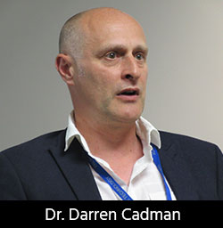
The final presentation came from Dr. Darren Cadman from the Compound Semiconductor Applications (CSA) Catapult, a government-backed not-for-profit technology and innovation centre aimed at helping the UK to become a global leader in developing and commercialising new applications for compound semiconductors through collaboration both with large companies and with start-up operations. The CSA Catapult is focused on sub-system and system optimisation and the development of tools and techniques to facilitate manufacture of product. Cadman explained that a compound semiconductor, composed of chemical elements belonging to two or more different groups in the periodic table, has unique material properties that offer many advantages over silicon, principally in terms of electron mobility, resulting in much faster processing speeds while consuming only a fraction of the energy. In power electronics and radio frequency systems, compound semiconductor devices can enable significant improvements in performance, size, weight, cost, and power. And in photonics, the distinctive emitter and detector functions of compound semiconductors provide much enhanced sensor capability. Cadman considers compound semiconductors to have the potential to drive the next wave of advances in telecommunications, robotics, renewable energy, and autonomous vehicles. Taking the telecommunications sector as an example, he stated that the Paris Agreement requires a halving of greenhouse gas emissions by 2030 and the UK had set a target of a 68% reduction from 1990 levels. He explored the benefits of an energy-efficient network in reducing carbon footprint, operational expenditure, and energy security. In a wireless cellular network, 73% of the total power consumed is associated with base stations, where power amplifiers are the dominant component with regard to power consumption, and the majority of the power used is wasted in the form of heat. The inefficiency is influenced by signals with a high peak-to-peak energy power ratio, which he illustrated graphically. The transition from 4G to 5G would require 10x more cells because of the shorter effective range of the higher frequency signals, and a shift from large central base stations to smaller local stations with power amplifiers based on gallium nitride operating at higher voltage, frequency and temperature. The CSA Catapult addresses the consequent thermal management and packaging challenges, toenhance functionality and performance while reducing cost and size. Cadman showed examples of the extensive equipment resources in its packaging facility. A further technology development he discussed was hybrid wireless bonding and interconnection of semiconductor chips using micro-bump techniques, including the UK’s first open-access, sub-10 micron hybridisation capability, together with facilities for additive manufacturing, PCB prototyping and 3D embedded packaging. |
|
In his closing comments, Bill Wilkie thanked all who had contributed, with a special mention of the table-top exhibitors, and remarked that he never ceased to be surprised at the breadth and depth of knowledge that existed within the Institute. As an additional benefit, delegates had free access to the motorcycle museum, which houses the largest collection of British motorcycles in the world with over 1,000 machines from 170 different manufacturers. A wonderful nostalgia trip to end an excellent day. |
|
| Go back to Contents |