
The Institute of Circuit Technology Annual Symposium 2018

ICT technical director Bill Wilkie is well-known for choosing notable venues for Institute of Circuit Technology events, and his choice for this year’s Annual Symposium was the National Motor Museum, located in the village of Beaulieu in the heart of the New Forest, a national park in the county of Hampshire in Southern England.
The region is known for its heathland, forest trails and native ponies. The museum houses a collection of around 250 vehicles manufactured since the late 1800s and was established in the 1950s by Lord Montagu of Beaulieu as a tribute to his father, a pioneer of motoring in the United Kingdom.
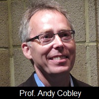 Introduced by ICT chairman Professor Andy Cobley, the principal theme of the symposium was advances in digital imaging technology, and he welcomed a distinguished audience of delegates that epitomised the “Who's Who” of the UK PCB industry.
Born locally, Professor Cobley was proud of the industrial heritage of the area, making particular mention of Supermarine Aviation Works, the aircraft manufacturer that produced the Supermarine Spitfire fighter as well as a range of seaplanes and flying boats and the engine that powered the land-speed record-breaking Golden Arrow.
He took the opportunity to give an update on the progress of the Maturolife project, led by his team at Coventry University and aimed at producing an innovative assistive technology with sensors integrated into fabrics and textiles. Key objectives were to develop a method for selective metallisation of textiles, and to replace traditional palladium catalyst with a lower-cost copper nanoparticle catalyst. A copper nanoparticle catalyst produced at Coventry University had been successfully used in the electroless copper plating of polyester fabric.
 Professor of Intelligent Systems at Loughborough University, Andy West gave the keynote presentation, focused on Industry 4.0 in electronics manufacture. His multi-disciplinary Embedded Integrated Intelligent Systems research group at Loughborough was engaged in a wide range of projects developing the tools, methods and value of applying adaptive embedded systems in manufacturing, healthcare and sport. “What you put into the digital space has to link to some sort of knowledge that makes the business run better!” He stressed that information and communication tools were strategically important key technologies to enable current and next generations of manufacturing, and that knowledge management and methodologies were required to support design through to production with embedded intelligence, continuing through operational life and service and eventually end-of-life and re-birth into new products and processes.
Professor West referred to the study, commissioned by the IMPULS Foundation of the German Engineering Federation which offered an on-line self-check to determine a company’s level of readiness for Industry 4.0, identifying areas where it was already well prepared, and where there was room for improvement. The 4th Industrial Revolution was based on cyber-physical systems and Professor West gave many examples of control and monitoring by embedded sensors and actuators, interactions between physical and software components, advanced analytics, visualisation and prediction algorithms.
His group was very keen to cooperate with industry and had worked closely with an automotive manufacturer on the implementation of intelligent systems, finding it preferable to work in a factory environment rather than a laboratory in order to get closer to reality and achieve more rapid feedback of meaningful observations. The group had also experimented with embedded RFID and sensors in PCBs and SMT assembly equipment as a demonstration of intelligent systems in electronics manufacturing.
A specific example of a project that presented a business opportunity with environmental benefits was a novel cyber-physical system providing flexible, adaptable control of the refurbishment of waste electrical and electronic equipment, mobile phones in this instance. The outcome was visibility of traceability and process data for customer and processor, confidence that the end user got a working device, confidence for the supplier that sensitive data had been erased, and confidence for the processor that maximum value had been extracted.
 “Fast and Fine” was the title of the presentation by Neil Chamberlain, Polar Instruments’ European sales manager, who discussed the signal integrity challenges of fine lines and high-speed signalling. He emphasised the significance of copper profiles and conductor geometry in high-speed applications. Whereas at the 50–60Hz frequencies typical in electric power transmission the cross-section of the cable was calculated to minimise energy loss through resistance heating, signal lines operating at GHz frequencies exhibited a “skin effect,” where most of the signal was carried in a thin surface layer of the conductor. For low frequencies the skin depth was several millimetres, but for example at 2GHz, it was as little as two microns. “Most of it is carried in the roughness!” he declared, referring to the bonding treatments applied to electrodeposited copper foil during its manufacture and during multilayer PCB fabrication. To illustrate this, he quoted the IPC definition of roughness for very-low-profile foil (5.2 microns maximum), and ultra-low-profile foil (no maximum stated but typically about 2 microns).
The PCB designer needed the facility to simulate roughness with an effective modelling tool. With reference to the assertion of George P. Box: “All models are wrong, but some are useful,” Chamberlain commented that even the best modelling tools were of no use unless the designer could incorporate some meaningful numerical values. He described the 3-D “pile of cannonballs” concept developed from the “snowballs” theory demonstrated by Paul Huray, to predict the additional power losses associated with copper roughness, which gave good correlation with observed measurements for rough microstrip lines. But there remained the need for a known standard, and Chamberlain cited Segal’s Law: "A man with a watch knows what time it is. A man with two watches is never sure." The fallacy was that the man with one watch could not be sure he knew the right time unless he had a standard to compare it with, because otherwise he had no way of identifying error or uncertainty. And the same applied in the case of the man with two watches—unless he had a point of reference, there were risks in making decisions based on conflicting information.
Chamberlain demonstrated the differences in insertion loss figures obtained by different modelling methods and commented that when lines were very fine or very long, the DC resistance of the line could not be ignored when measuring its true impedance. A technique known as Launch Point Extrapolation could now be used to compensate for the effects of series AC and DC resistance and achieve a closer match between lossless field solver models and measurements on thin copper or fine line PCBs.
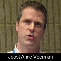 Neil Chamberlain’s presentation set a scene for Joost Anne Veerman, MuTracx International’s inkjet printing specialist, to discuss the results of an investigation of the effects of conductor edge smoothness on impedance. Veerman explained how a conductor image was created as a composite of a series of ink droplets and demonstrated the characteristic differences between X-direction and Y-direction features. The nature of the inkjet process was that, however accurately it was controlled, the edges of features would always show some evidence of waviness as a consequence of the residual geometry of successive drops. By comparison, direct imaging with a photoresist resulted in more sharply-defined edges. To some extent, the etching process has a smoothing effect, but there remained a distinct difference in conductor-edge geometry between the two technologies. The questions to be resolved were whether this difference was significant in the context of controlled impedance and whether inkjet imaging was appropriate for high frequency PCBs.
A test board had been designed using a composite of standard IPC coupons in 0°, 45° and 90° orientations in a 10-layer stack-up, featuring 100-ohm edge-coupled differential strip-lines with 100/150 micron and 100/100 micron track/gap, and single-ended strip-lines with 175 micron 50 ohm, 75 micron 75 ohm, and 195 micron 50 ohm tracks.
Two panels were manufactured using the MuTracx inkjet printer, and two using LDI and photoresist. Track widths and edge waviness were measured on innerlayers before and after etching. Impedances were measured with a time-domain reflectometer, and microsections were made for measurement of dielectric and copper thickness. Veerman showed comprehensive test data.
From the results it was clear that there was no strong correlation between cross-section data and impedance. Impedance correlated with average track width and, significantly, no difference was observed between LDI and inkjet imaging technologies in terms of the effect of track-edge waviness. Dielectric thickness had the most dominant effect, together with the effect of resin-to-glass ratio on dielectric constant.
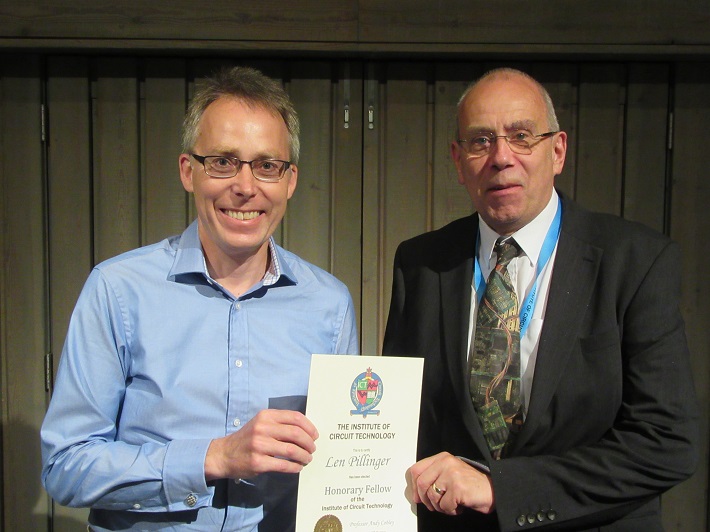
Before the commencement of the afternoon session, the indefatigable efforts of Len Pillinger over many years of acting as the link between the Institute and the standards committees were recognised in the award of Honorary Fellowship, presented by ICT Chairman Professor Andy Cobley.
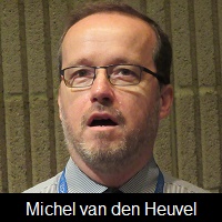
The programme re-commenced with a discussion of advances in direct imaging technology from Michel van den Heuvel, imaging group director at Ucamco.
 The programme re-commenced with a discussion of advances in direct imaging technology from Michel van den Heuvel, imaging group director at Ucamco.
The trend had been to move from high-pressure mercury lamps to UV-LED light sources, particularly for solder mask exposure. The state-of-the-art was a broad-multi-wavelength system, with peaks typically at 365, 385 and 405 nanometres, operated simultaneously and with the ability to control individual intensities to optimise the mix to suit individual solder masks.
The shorter wavelengths favoured the polymerisation of the surface of the solder mask, the medium wavelengths penetrated deeper into the thickness, and the longer wavelengths ensured good polymerisation at the copper surface. The optimised combination gave a very uniform through-cure, resulting in very straight sidewalls after development and the capability to reliably resolve 50-micron solder dams without undercut, as well as shortening the exposure time and hence increasing throughput. The system also gave very good results with black solder masks. Van den Heuvel explained that the Ledia equipment supplied by Ucamco had many advanced features: its autofocus capability could compensate for panel warpage of up to 800 microns; its automatic imaging-head calibration facility ensured the position of each imaging head in relation to the other five heads, resulting in perfect stitching of the image and compensated for minute dimensional changes in the machine due to temperature variations. It also had a range of innovative automatic alignment features to compensate for substrate distortion. To fulfil the requirement for complete traceability, there was the facility to mark every individual PCB image with a unique identity, human- or machine-readable, which could also incorporate scaling information if required.
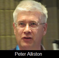 Peter Alliston, VP sales for Orbotech West, discussed the trends currently driving PCB technology, and described how leading suppliers of imaging and inspection tools had responded with developments in the capability of their equipment. He identified four market sectors: Internet of Things and 5G infrastructure, smartphones, automotive, and Industry 4.0 and robotics.
High-frequency PCB designs for 5G wireless broadband operating in the millimetre wave spectrum would demand strict impedance control at the 5% tolerance level, and low-loss materials. It was forecast that there would be 30 billion connected devices by 2020 and 75 billion by 2035.
Smartphones were leading mass production technology, with trends to 20X faster processing and communication rates together with increased battery capacity, to support augmented reality, artificial intelligence, and biometric and medical sensing. As batteries got larger, the space available to accommodate the PCBs got smaller, forcing an increase in interconnection density towards 20-micron lines and spaces that could not be achieved by established HDI processes. The technology was trending towards substrate-like-PCB (SLP), produced by modified semi-additive processing (mSAP). The use of flex in smartphones was increasing—up to 20 flex circuits in every unit, and there was a move towards roll-to-roll manufacture for more cost-effective production
Rapid development continued in automotive electronics, and the requirements of safety and autonomous operation were driving advances in sensor technology—radar, lidar, cameras, long range radar, and ultrasonics, many of which needed 5G connectivity. The use of HDI was increasing, and the automotive sector was forecast to represent 15% of the total HDI market by 2020.
Enormous investment was being made in automation, smart data exchange and cyber physical systems, and the global robotics industry was forecast to expand from $34 billion to $226 billion by 2021.
So how did a company like Orbotech respond to these trends and provide solutions for the PCB industry? Alliston described latest developments in direct imaging for HDI, mSAP and solder mask, with particular emphasis on achieving registration accuracy and high throughput. He discussed new concepts in AOI with integrated 2D metrology, and how the needs of Industry 4.0 were supported with a smart factory metrology package offering full product traceability for root cause analysis and life cycle control.
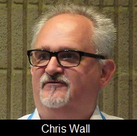 Chris Wall, technical director of Electra Polymers and ICT Treasurer, discussed inkjet as a method of patterning solder mask. Speaking from over three decades of experience in ink formulation, he began by defining the performance requirements of a solder mask, a permanent polymeric coating for a printed circuit board, patterned to allow access to selected areas of copper, and resistant to subsequent processes and to the end use environment, preventing the growth of metal whiskers and preventing corrosion of underlying circuitry. Its primary purpose was to enable mass soldering processes.
There were two principal process routes to creating a solder mask pattern: indirect and direct. The indirect route involved coating all over with a photoimageable material, exposing an image using a photomaster or a laser, developing to remove unexposed material, and final curing. The direct route was to place the material only where it was needed, traditionally by screen printing, or more recently by inkjet printing, followed by a final cure.
The intrinsic limitations of screen printing were resolution and registration, plus the need to make and store artworks and screens. Drop-on-demand inkjet offered a repeatable digital process with potential for high output, with the capability to scale and offset the image to compensate for distortion of the PCB. Reduced waste, reduced energy costs and reduced work-in-progress were other potential benefits. But how to formulate an ink that would jet successfully and meet the material performance requirements?
Wall described the piezoelectric drop-on-demand process and demonstrated how a drop was created and how it could change its shape in flight. The tail formed as it left the nozzle could be absorbed into the drop or could break away as a satellite and be deposited as an extraneous pattern defect. Formulation of inkjet solder masks was subject to several constraints, and there were a limited number of suitable raw materials. The choice was restricted to very low-viscosity resins and monomers, with low or no filler content and pigment particle sizes less than 200 nanometres, compared with 5–15 microns for conventional solder masks. These low filler contents could adversely affect flammability, thermal shock and solder resistance. And the low viscosity and surface tension meant that good jetting performance was constrained by the laws of physics and the type of print head used. There could be a tendency for pigment sedimentation on storage and to spreading, bleed and track edge thinning on printing, with performance heavily dependent on surface preparation.
The mechanism of curing depended on the resin chemistry. UV-cured acrylates polymerised and cross-linked by a free radical chain reaction, epoxies by a cationic reaction, and hybrid epoxy/acrylate systems by a combination of the two. It was normal practice to additionally carry out a final thermal cure.
To help overcome bleed and track edge thinning effects, the ink could be instantaneously pin-cured with low-level UV to fix droplets in place, and multi-layered techniques could be used to initially create dams around pads before subsequent filling to eliminate striping, build up thickness on conductor edges, and give a smooth ink surface with sharper edge definition. Specialised surface treatments could be used to minimize the spread of ink droplets.
Chris Wall made the closing remarks on behalf of the Institute, thanking speakers and delegates for making the event another superb learning and networking opportunity, Bill Wilkie for pulling it all together, and Polar Instruments for their generous support. And to round off the day, everyone had the opportunity to browse one of the finest collections of cars, motorcycles and motoring memorabilia in the world.
June 18, 2018 | Pete Starkey, I-Connect007