
Journal CSS

The Journal of The Institute of Circuit Technology Vol 13 No 2 September 2020 |
|
| Links to Contents |
Section |
| 1 | |
| 2 | |
| 3 | |
| 4 | |
| 5 | |
|
ReCollect - Efficient Manufacturing of Recyclable Composite Laminates for Electrical Goods |
6 |
|
Shrinking Medical Labs onto Printed Circuit Boards for Disease Management |
7 |
|
Fully Biocompatible Dry Film for MEMS, Lab-on-chip, Microfluidic, Medical Devices. |
8 |
| 9 | |
| 10 | |
|
Industry News: Adeon, Amphenol-Invotec,Atotech, Eurotech, Merlin, Minnitron and Ventec. |
11 |
| 12 | |
| 13 | |
| Section 1 |
Calendar of Events |
| Date | 2020 Events |
| 25th February | AGM and Evening Symposium |
| 6th - 9th April | Annual Foundation Course - Chester - POSTPONED |
| 2nd June | Annual Symposium at the British Motorcycle Museum - POSTPONED |
| 8th September | Autumn Seminar -Tewkesbury POSTPONED |
| TBA November | Winter Seminar - Hartlepool |
| 2021 Events | |
| 25th February | AGM possibly by Zoom Meeting |
| Section 2 | An Industry Changed Forever |
|
Editorial Matthew Beadel Technical Director, |
When I was asked if I would write an editorial for the latest edition of the Journal, I did not have to think for long about what I should say. In my ‘near’ 30 years in the industry I have experienced many key events including a couple of recessions, Site closures, ROHS, migration of mainstream business Offshore and even the advent of digital imaging – to name a few. All have in their own way had an impact on the industry, both positive and negative. Since joining the industry in the early 90’s, the UK PCB industry has unfortunately reduced and needed to evolve many times – creating its own opportunities when none were given to it. But now we have been presented with maybe the greatest challenge ‘COVID 19’, it has changed everything from the phrases we use, Social distancing, shielding, the R no. to the way we interact internally and even how we meet with others. No longer driving long distances, meeting in airport lounges or cramped conference rooms - it is all Zoom or teams from the office or on the couch at home, ensuring the backdrop is not to messy! – maybe not all bad then. Not to ignore the devastating personal effects of the pandemic on many people’s lives, but it has also ‘I believe’ changed our industry forever. At first many PCB companies adjusted their core business to support calls for medical PCB’s for Ventilators, monitoring devices etc - for many at the expense of their core customers. The staff working crazy hours – some facilities not shutting for 2 months straight and breaking output records. But once the medical requirement reduced there was then the realisation that some of the customers who these companies relied on, consumer, Automotive, Aerospace etc were either closing or reducing stocks levels so orders slowed. A few manufacturers were helped by product coming back from the Far East ‘Re-shoring’ but will this last, unlikely as money talks. So now is again a time for our industry to evolve, look for new markets or re-investigate forgotten ones. There may be casualties along the way, but I do feel as an industry we will adapt and move forward – we are a very resilient bunch. This will be assisted by the ICT and the tireless work that the council do for our sector, not to forget the recently formed Fabricators group which gives the members a much louder combined voice and helps facilitate manufactures to help each other - which is more important now than ever before. So, looking forward I believe there is still a place for the UK PCB Industry, maybe looking slightly different, leaner but still leading the way in innovation whatever the future holds. Mathew Beadel September 2020. |

| Section 3 |
ICT Council Members |
| Council Members 2020: |
Emma Hudson (Chair), Andy Cobley (Past Chairman), Steve Payne (Deputy Chairman), Chris Wall (Treasurer), William Wilkie (Technical Director, Membership & Events), Richard Wood-Roe (Web Site), Lynn Houghton (Hon Editor), Matthew Beadell, Martin Goosey, Maurice Hubert, Lawson Lightfoot, Peter Starkey, Francesca Stern and Bob Willis, |
| Section 4 | Membership News | ||
|
4.1 David Clayton |
Obituary - David Clayton Sadly, David Clayton, one of our founder members, passed away last year. In the absence of a formal eulogy Alun Morgan has prepared a short piece to recognise his passing. David Clayton – A personal reflection I first met David in 1980 at Nevin Electric in Colnbrook where I was attending a job interview. All started well but David began asking increasingly difficult questions about PCB technology, which was a subject I knew very little about being employed at the time as a Research Investigator mainly concerned with non-destructive testing. After a while and sensing my unease, David said “You are here for the job as Technical Manager, aren’t you?”, I replied, “No, I came for the job as works plating chemist”. David took stock and said “Okay, let’s start again!”. That summed up David, whatever situation he faced, he was always pragmatic and found a way forward, very few situations would faze him. Having begun the interview again, but this time with appropriate questions, David realised that my metallurgy degree had equipped me with some knowledge of electroplating and he ended up offering me the job of Technical Manager designate. David was an old school engineer, he loved making things. He told me that in his younger years he couldn’t afford to buy a car, so he decided to make one from scratch. He succeeded, but in order to get a road worthiness certificate he had to give his creation a name, he chose to name the car the “Clayton Special”. During my time working with him I discovered that his engineering prowess wasn’t limited to cars and many “Clayton Specials” could also be found at Nevin where David had turned his hand to solving engineering problems in his own unique way. We used to make regular trips together in David’s Mercedes estate car to the Nevin Lonsdale plant in Waterlooville to “help” solve problems, we normally succeeded but I’m not sure we made too many friends there after having pointed out on one occasion that anode bags were supposed to contain metal anodes and not sludge! David’s Mercedes was quite famous as it was featured driving under a motorway bridge on a TV road safety advert from the 1980s. The other claim to fame is that David and I sold a quantity of scrap circuit boards to the production company for “Superman 3” which was being filmed at the nearby Pinewood Studios. The boards were used to build Superman’s computer and can be clearly seen in the movie. David tried to negotiate a mention for us in the film credits, sadly unsuccessfully! I have a lot to thank David for and as one of the founding fathers of the ICT and Chairman from 1986-1988 we all owe him a great and lasting debt of gratitude. Alun Morgan
|
||
| 4.2 | Membership Update | ||
|
Bill Wilkie
Technical Director and Membership Secretary
|
MEMBERSHIP NOTES The Covid crisis has meant that we were unable to hold our Annual Foundation Course this year. This was doubly disappointing in that 2020 is the 40th anniversary of the course and we meant to honour this fact throughout the year. We decided to send framed commemorative certificates to all companies who had supported the course, either by sending lecturers, delegates, or enabling venues and we completed the project last month. It’s not well known that completion of the Foundation Course is accompanied by a presentation ceremony, where delegates are presented with Associate Membership certificates, usually by the Institute Chairman. The council decided that in this anniversary year, it would try and support prospective delegates by awarding Associate membership for a two-year period to delegates unable to attend due to the cancellation of the Course.
|
||
| Memb No. | Fellows | ||
| 10477 | Philip Johnston | Trackwise | |
| 10478 | John Priday | Teledyne Labtech | |
| Associate Members | |||
| 10478 | Silver Merkoci | Sun Chemicals | |
| 10479 | Zbigniew Polak | Eurotech Group | |
| 10480 | Ryan Kyle | Eurotech Group | |
| 10481 | Jason Price | Eurotech Group | |
| 10482 | John Gover | Eurotech Group | |
| 10483 | Matthew Baines | GSPK Circuits | |
| 10484 | Lewis Wrigglesworth | GSPK Circuits | |
| 10485 | Elana Neascu | Circuit Foil | |
| 10486 | Gauthier Gerardin | Circuit Foil | |
| 10487 | Michelle Hunt | ALR Services | |
| 10488 | Matt Webb | ALR Services | |
| 10489 | Alex Scawn | Lyncolec | |
| Go back to Contents | |||


| Section 5 |
Smart PCB Material Selection for Smart Design ResultsAlun Morgan |
Alun Morgan Technology Ambassador, Ventec International Group |
New-product designs today not only have to achieve ever greater performance, but the PCB designers behind them are increasingly working under intense commercial pressures like never before. Choosing the right substrate materials therefore is more important today than it has ever been. With a wide selection of materials available that offer ever more finely nuanced properties, making the right choice is not an easy task. Fortunately, suppliers and industry bodies offer some guidance, but designers can also help themselves by being more willing to share information with their suppliers. Closer working partnerships are key for us to be more open from a technical standpoint if the next generations of high-tech products are to meet the world’s future needs. Complex, performance-hungry technologies like 5G and AI simply must succeed if we are to have the foundations necessary for smart living: smart energy, smart cities, smart buildings, smart factories, smart healthcare etc. will be essential to ensure a high quality of life for us all whilst at the same time preserving the planet’s resources. Typically, of course the board is the last part of a project to be specified when a new product is being designed. On the other hand, it’s the first item to be needed when serious development begins. Designing the circuitry to go on the PCB quite rightly gets most of the attention and the substrate itself is usually the lowest priority in an engineer’s mind. When the time finally comes to consider it, design teams will often simply default to using the same materials as were used previously. As the performance demands imposed on successive product generations continue to intensify, and factors such as conductive anodic filament (CAF) formation that seriously affect reliability become more critical, this approach is increasingly risky. As the industry has come to understand more about how the substrate properties influence performance and reliability under various operating conditions, so the number and diversity of material types on offer has increased. In the past there have been only a handful of options open to designers. Today, international specifications offer over 100 different material categories to choose from. Designers, understandably, struggle to connect the specifications with the properties they are looking for. It doesn’t help that these specifications are usually based on chemical composition. As the breadth of choice on offer continues to increase, it’s almost impossible for electronics engineers to relate to them. Suppliers such as Ventec are therefore moving to performance-centric specifications that are easier for engineering communities to interpret. Getting help is essential, because struggling on alone risks under-specifying or over-specifying the material for the application at hand. Neither is good: under-specifying risks the product coming up short in a way that could be beyond any realistic remedy. Over-specifying, to be “on the safe side”, can be commercially disastrous in ultra-competitive markets such as consumer technology. The chosen materials also need to be readily available in any location globally where the product is to be manufactured. Some resins, for example, are only available in certain domestic markets and are difficult to procure elsewhere. Designers can also take advantage of another emerging trend among suppliers, which is to present carefully curated sets of materials for specific application areas. Ventec’s autolam and aerolam material guides (aerolam is launching soon), for example, bring together products with properties suitable for automotive or aerospace and further sub-divide them according to target applications and operating environments, such as under-the-hood or in-cabin. In this way, companies like Ventec effectively contribute their expertise to help customers shortlist products that can meet their requirements. This helps by simplifying and accelerating selection, narrowing the focus onto materials that are fundamentally suitable. Helpful though this is, as suppliers we often need designers to express their requirements directly if we are to provide the right material for the right task. Being too sparing with information, particularly about the intended application and operating environment, risks having to recall large numbers of units from the field. With just a little more willingness to share information, the problem can be avoided rather than demanding a remedy that is both financially and reputationally expensive. While it’s understandable for any OEM to be wary of sharing information about their intellectual property and product strategies, the value of trust between OEMs and their supply partners is paramount. As the issue of materials selection becomes more complex and, at the same time more important to get right first time, there is increasingly more to gain by finding ways to be open and more to lose by keeping traditional barriers in place.
Alun Morgan, Technology Ambassador, Ventec International Group |
| Section 6 |
Institute of Circuit Technology Dissemination Newsletter July 2020 Bill Wilkie |
||
|
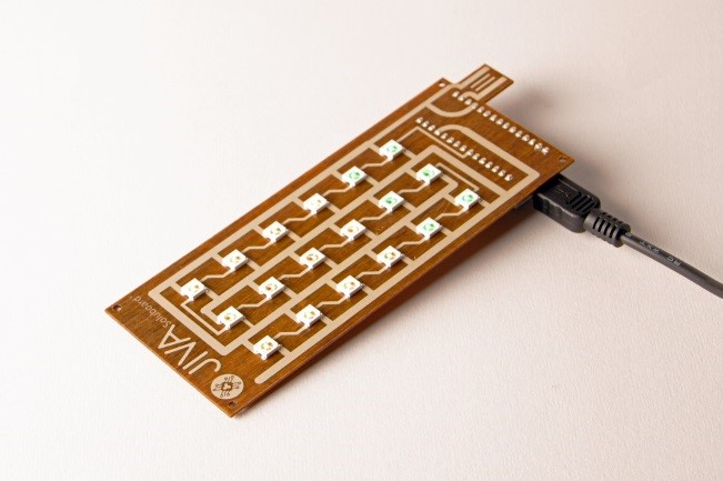
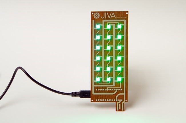
The Institute of Circuit Technology is the dissemination partner for "ReCollect". A grant funded project to demonstrate the feasability of manufacturing a fully biodegradable and non-toxic PCB laminate |
ReCollect - Efficient Manufacturing of Recyclable Composite Laminates for Electrical Goods – No 34163
The ReCollect project is funded by Innovate UK, part of UK Research and Innovation. It began in October of 2019 and is intended to run for 30 months. Normally, the ICT would be holding events which could be used to disseminate the latest information on the project, but during the Covid-19 lockdown, we are using this on-line vehicle to ensure that the Industry is kept up to date.
Innovate UK is the UK’s innovation agency. Innovate UK works with people, companies and partner organisations to find and drive the science and technology innovations that will grow the UK economy - delivering productivity, new jobs and exports. The aim at Innovate UK is to keep the UK globally competitive in the race for future prosperity.
PARTNER ORGANISATIONS: LEAD PARTNER Established in September 2017, Jiva Materials Ltd is a sustainability start-up based in London, UK. Coventive Composites is a specialist independent consultancy, providing technical expertise and access to pilot-scale equipment and testing facilities to help our clients develop and commercialise novel composite materials and components. Our expert advice and technical support cover all aspects of the product development lifecycle. The ICT facilitates dissemination of knowledge and expertise by a series of seminars and symposiums in varying locations throughout the UK. The ICT Quarterly Journal contains papers and information regarding novel processes and techniques and they also offer an annual Foundation Course in PCB manufacture and design. This is a valuable source of information for both novices and more advanced engineers wishing to widen their knowledge and experience of the application of cost effective and reliable processes and techniques.
Review of progress at our last evening event At the end of the second quarter, Dr Jonathan Swanston, chief technical officer with Jiva Materials, gave an update on the ReCollect project and explained the background to the development of the world's first fully recyclable PCB laminate. He passed-around samples of his material, composed of a natural fibre bound with a polymer soluble in hot water but not in cold water, which had the appearance of a light-brown-coloured unclad laminate. Dr Swanston reviewed some statistics which indicated that PCBs made up 8% of the 50 million tonnes of electronic waste that was generated in 2018. The ReCollect project explored an alternative way of managing end-of-life circuit boards. Currently, the only practical way of recycling glass-epoxy circuit boards involved shredding and incineration to recover the metal content. The ultimate aim of the project was to remove glass-epoxy boards from the supply chain, by demonstrating that Jiva’s Soluboard® could match the performance of CEM-1 and FR-4 materials. He explained that Soluboard® was a fully biodegradable and non-toxic product based on flax. A primary aim of the project was to demonstrate the feasibility of producing the material in high volumes at a competitive price, using a continuous-production process in development by Coventive Composites. The nature of Soluboard® was to delaminate when immersed into hot water, enabling the flax fibres to be composted or repurposed and the electronic components to be removed for re-processing. Silver printing was a feasible method of creating functional circuits, but in order to use existing aqueous manufacturing processes it was necessary to seek a means of chemically protecting the material in-process, and this was part of the project. Dr Swanston commented that “white goods” – large household appliances – constituted more that 30% of e-waste, and that the Global E-Waste Monitor had reported that less than 20% of this was documented as collected and recycled. The rest went to landfill. Jiva intended to push for the safe recovery of e-waste in line with the WEEE2 Directive. The white goods market was their initial target, and specifications from potential customers had defined electrical, flammability and mechanical requirements. Soluboard® had a Tg of 126°C and a UL94V0 flammability rating. Its electrical properties were being determined by a third-party laboratory and final results were awaited. As part of the project, functioning populated PCBs would be designed, manufactured and evaluated as specified by end customers.
We intend to update this newsletter as a monthly link to our website as a way of keeping the project in the Industry's in-tray, during the lockdown. |
||
| Go back to Contents |
| Section 7 |
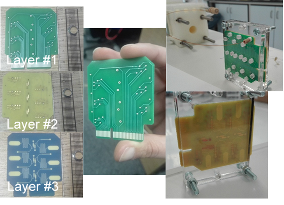
Shrinking Medical Labs onto Printed Circuit Boards for Disease ManagementDespina Moschou |
|
Dr Despina Moschou C3Bio, Electronic and Electrical Engineering, University of Bath, UK Dr Moschou is an Assistant Professor at the University of Bath, UK, developing innovative biomedical diagnostic Lab-on-Chip devices for the past 7 years. She is also co-founder and Managing Director of the medical diagnostics start-up biotIP Ltd. |
“Our key message is: test, test, test”. This quote by the head of the World Health Organization during the ongoing COVID-19 outbreak sums up a major challenge for global public health: we can’t fight fires blindfolded, whether the case is a novel virus pandemic, water contamination or personalized disease treatments. But is it realistic to expect healthcare systems to cope with this increasing demand for ad-hoc diagnostic testing? As clearly demonstrated, there will always be a limit to our capacity of laboratory facilities, equipment, technicians and reagents. Additionally, diagnostics are continuously evolving to meet emerging needs: new pathogens, new biomarker combinations, new environmental applications, personalized biomarker panels. A viable way to cope with such a broad and dynamic demand is if everyone had access to their individual laboratory.
In our research group we have focused in the past 10 years in developing commercially manufactured, seamlessly integrated Lab-on-Chip devices via Printed Circuit Board Technology, pioneering a new research area named Lab-on-PCB devices. The feasibility of such devices has been proven for a wide variety of clinical applications (sepsis, types of cancer, diabetes) and currently being explored also for the rapid diagnosis of SARS-CoV-2 at the community level. It is realistic to believe that the following years will see a more widespread commercial development of such systems, stemmed by the renewed public health interest globally, so make sure to watch this space!
https://en.wikipedia.org/wiki/Lab-on-a-chip https://www.nature.com/nature/journal/v442/n7101/full/nature05058.html http://pubs.rsc.org/en/content/articlelanding/2017/lc/c7lc00121e#!divAbstract |

 This level of democratization may seem far-fetched, however, it is not unprecedented: integrated circuits (ICs) enabled the miniaturization of mainframe computers and thus forever transformed the world, democratizing information to a degree unimaginable until then. With the invention of the IC, computing power was not limited in specialized scientific laboratories anymore, reaching the point where every person in the world is holding a supercomputer in their hands. A multitude of new professions have been created to develop ICs and high-tech electronics, packing in little black boxes sophisticated expertise, used daily by end-users with no scientific background. This is precisely the challenge that Lab-on-Chip technology aims to address: offering more detailed, automated, stratified and rapid medical diagnosis to patients, by shrinking complete biomedical laboratories in few cm microchips. The advantages of miniaturization and stratification of technology have already been demonstrated by the computer revolution of past decades: originally mainframe computers used to take up whole rooms, and thus allowed access to information processing only to the few experts. When processors got miniaturized in few cm microchips the world changed: we got PCs/laptops/smartphones, information was democratized and allowed every person in the world access to the digital world.
| Section 8 |
Fully Biocompatible Epoxy Acrylate Dry Film for MEMS, Lab-on-chip, Microfluidic and Medical Devices. Giorgio Favini |
|
Giorgio Favini CEO, Elga Europe |
Introduction Elga Europe s.r.l. is an Italian company established in 1973 and it is the only dry film producer in Europe since 1995. During the first years of 2000 the company expanded its marker all over Europe and reached more than 75% in 2013, after the joint venture with Eternal Materials (which absorbed Elga Europe in its holding in 2015). Elga Europe has its own internal R&D lab where, thanks with very strict contact with the customers and the market through technical support, is able to create new formulation in order to “keep pace with the times”. An example is the develop in 2013 of the only dry film on the world market with 60µm thickness suitable for pure 405nm wavelength exposure machines. The company has also a dedicate production plant for ultra-pure developer solution for semiconductor industry and a copper foil slitting plant. Moreover, in collaboration with Resistechno as exclusive distributor, Elga Europe produce and commercialize a fully biocompatible dry film for MEMS, lab-on-chip, microfluidic, medical devices. Those different product types allow Elga Europe s.r.l. to cover different business areas and work for special project as research for the future.
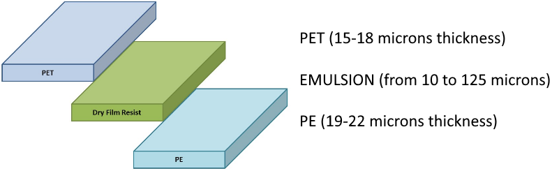
SY300 Dry Film Description The dry film is an emulsion of acrylate polymers and monomers that cross-link through UV radiation, using a photo initiator, making the structure resistant for the different process steps. Depending on the recipe, the production process involves from 18 to 25 different raw materials divided between polymers, monomers, powders and solvents. The materials are mixed, filtered and pumped into a coating plant; this plant is able to spread the emulsion (resist) on a PET carrier with thicknesses from 10 to 125µm with a maximum tolerance of 1µm on a width of about 1.5 metres. The resist is subjected to a drying cycle in dynamic ovens until a certain amount of residual solvent is reached: now the product can be classified as a dry film. The next stage involves the lamination with a PE sheet that allows the winding in master rolls from where rolls of the dimensions requested by the customer will be cut. Fig 1 . SY300 Structure
Ordyl SY300, unlike conventional dry films, is epoxy-acrylate based and incorporates all the chemical-physical characteristics typical of this material. Moreover, for the type of resins used, SY300 proves to be bio-compatible. The application process of SY300 is extremely simple and quick, extremely predictable:
At the end of the process, after final firing, the material is durable and can also be used as an adhesive layer if coupled with another layer of material. The SY300 can also be used as a "sacrificial layer", i.e. removed after the photographic, exposure and development process before the final firing.
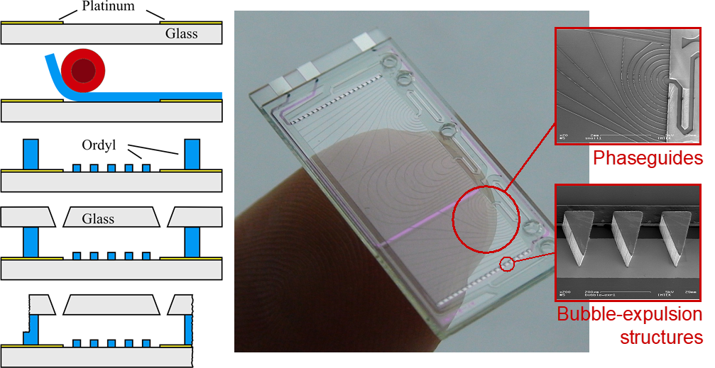
Key Features of Epoxy Acrylate Dry Films The SY300 finds application in various fields of use such as micro-fluid, photovoltaic, MEMS and thanks to its bio-compatibility also bio-MEMS and lab-on-a-chip where it successfully replaces liquid resistors traditionally used for these applications. The advantages of using a dry film instead of a liquid resistor are numerous:
Applications for Epoxy Acrylate Dry Film Here are some examples of applications of SY300 extracted from various scientific publications:
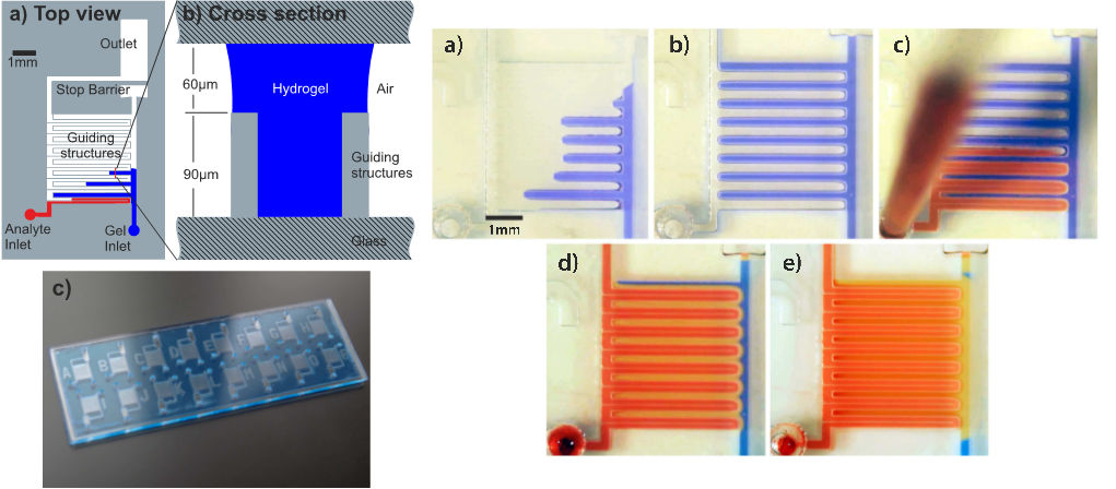
Fig 2 Lab On-Chip Acknowledgement:Vulto, et al., Lab Chip, 2010
Fig 3 Microfluidic Acknowledgement: Dietmar Puchberger-Enengl, Single-step design of hydrogel-based microfluidic assays for rapid diagnostics, Lab Chip, 2014,14, 378-383
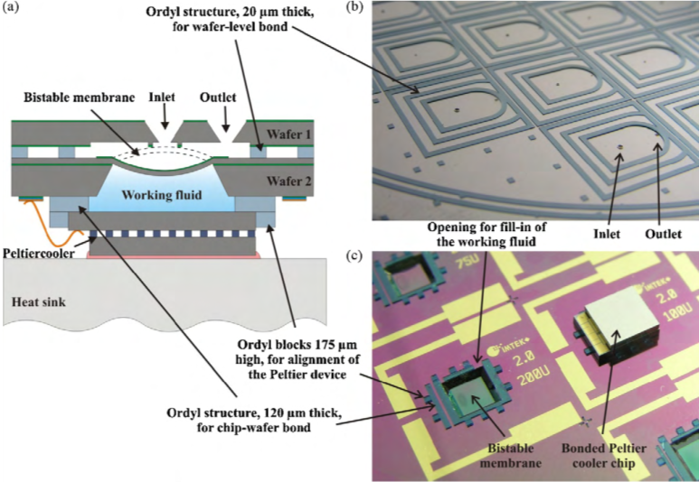
Fig 4 MEMS Acknowledgement: Huesgen et al. / Sensors and Actuators A 162 (2010) 137–144
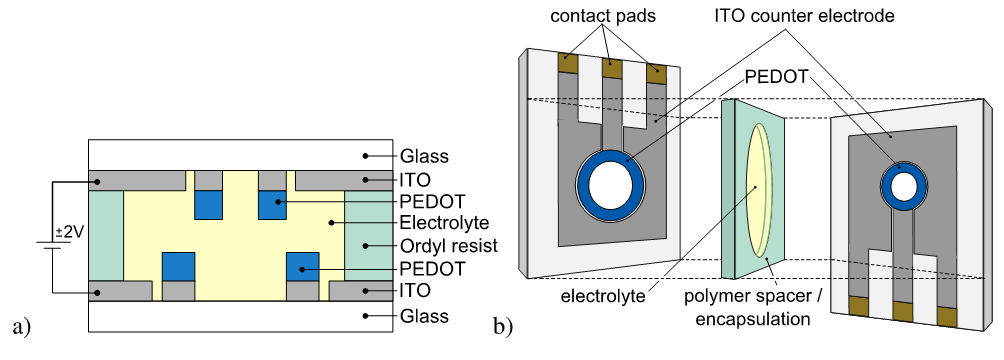
Fig 5. Bonding Acknowledgement: T Deutschmann et al., Integrated electrochromic iris device for low power and space-limited applications, J. Opt. 16 (2014) 075301
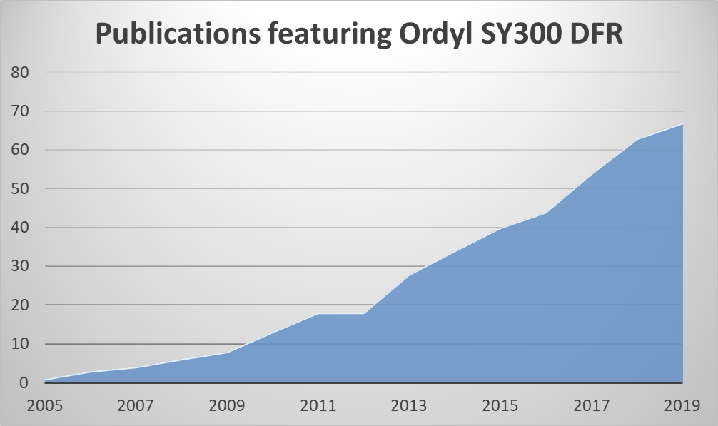
Fig 6. The number of publications related to the use of the Ordyl SY300 is constantly increasing, as the above graph shows: Source: Google/Scholar
For any further information, please contact Resistechno s.r.l., at |
| Go back to Contents |
| Section 9 |
IPC 6012 Medical Device Addendum for Printed Circuits |
|
Jan Pedersen Senior Technical Advisor at Elmatica
Jan has shared his knowledge of PCB at Elmatica since 1992, the last years as Senior Technical Advisor, solving thousands of engineering queries, securing the customers PCB design. He is also Chair of the IPC Medical Addendum group D-33AM, Automotive Addendum D-33AA and the IPC Automotive Initiative. Standards are close to his heart, always looking for improvements and further development. |
First ever Medical PCB Standard released - tightening the grip on compliance and data security
This summer the task group for the IPC 6012 Medical Device Addendum released the new IPC Medical Standard for Printed Circuits, after the idea was launched early 2016. The focus is on compliance, traceability and a new design level for printed circuits with a track and gap below 50 microns.
In 2016 Elmatica initiated a task group for Medical Applications. IPC accepted the challenge and founded IPC-6012 and 6013 Medical Addendum with Jan Pedersen as Chair. The IPC 6012 Medical Device Addendum passed the ballot after Industry review just before summer, now it's launched and ready to be implemented.
How is this standard standing out from other PCB related standards? Three key words can summarise how the IPC 6012EM stands out from other standards: Compliance, Traceability and Design level D. “All the three are equally important to meet the future expectations and increase the use of collective requirements instead of all the customer specific ones”, says Pedersen. When working on the standard the group faced some challenges with terminology. How to name different sections and PCBs, like Micro PCBs, and different Design Producibility Levels. “For the different design levels we had to suggest a completely new level due to the complexity for Medical Device Applications, the Level D. We analyzed all aspects and needs for medical devices. Identifying PCBs used in several applications such as implants and hearing-aids that have line widths, thickness, hole sizes and other features below current tolerances and limits in today’s Design, performance and acceptability standard”, says Pedersen. Imperfections in materials that would be acceptable in other industries, may cause application failures in Medical Devices, same goes for what test frequency waivers are accepted within the industry, all factors that needed to be analyzed and discussed in the Task Group.
Design Level D - track and gap below 50 micron Micro PBC was a terminology in need of a discussion and also the root cause forcing forward the new design level. For the IPC 6012EM the focus has been towards medical device applications with HDI design, also called Micro PCB, often found in hearing aids or pacemakers. “We see numerous PCB designs that are way below the standardized design levels, however there are many manufacturers producing them, still very few talking about it. It seems that many have the impression very few PCBs are produced with 75 micron track and gap. The truth is that quite a lot of the Micro PCBs are often below 60 micron, in fact many are way below 50 micron as well. This forced forward the need for a new design level - the design level D”, says Pedersen The IPC 6012EM is the first to address this terminology and the advanced design levels.
So what are the IPC Design Producibility levels? In the IPC-2220 series, IPC refers to Design Producibility levels of features, tolerances, measurements, assembly, testing of completion or verification of the manufacturing process, that reflect progressive increases in the sophistication of tooling, materials or processing, and, therefore progressive increases in fabrication cost. These levels are: Level A General Design Producibility – Preferred
The new proposed level suggested due to the complexity in the PCBs for Medical device Applications is called: Level D: Advanced Design Producibility – Exceedingly Reduced The producibility levels shall not to be interpreted as a design requirement, but rather as a method of communicating the degree of difficulty. Today these PCBs are made to customer requirements rather than following the IPC standard, this is not the path we want to continue on.
Traceability on all materials, processes and production of the PCB Another uniqueness about the standard is the focus on traceability in accordance with IPC 1782 level 4. This is strangely enough the first standard with demands for traceability to the PCBs on materials, processes and production. A feature Pedersen hopes and believes we will see incorporated in other standards as well. “With an increased focus on cyber security and documentation in many industries, like the new CMMC regulations in the Defence industry, the need for traceability is forced forward. This also flows down to PCB level. In an industry such as the Medical one, the need for reliability is crucial, thus also the ability to trace all elements in the PCB production”, says Pedersen.
Why is a digital specification the only way to go? This is why the Medical Addendum is the first to include the demand that to be able to secure compliance to product performance in the Medical Device Application, a computer readable Digital Specification shall be created during the product development process. The Digital Specification shall specify the product requirements in all printed board procurement stages between buyer and seller through the complete product lifecycle. “At Elmatica we say: Compliance in, is compliance out. With digitalization, AI and IoT, the traceability and transparency to where, by whom and how a PCB is produced will be even more important, compliance is on the map to stay and offers the ability to rule out the ones that don't follow the standard. This is why the Digital Specification shall be used in Request for Quotations to protect the buyer and secures that the seller has sufficient capability to meet the qualifications and requirements needed”, says Pedersen.
In what way will this standard affect the PCB Industry? “We are extremely content with the release of the new standard. Developing standards is a time consuming and detailed process, in particular for the Medical Industry, due to the complexity in Medical PCBs”, says Elmaticas Chair of the Medical Addendum Task group”, Jan Pedersen. With the new standard, the designers and manufacturers of PCB for medical devices can rely on specific parameters and requirements for production, which again will increase the reliability and transparency.
The purpose of this specification is to provide requirements for qualification and performance of Printed Boards for High Reliability Medical Device Applications. This specification covers Rigid Printed Boards that may have a design that contains HDI and Design Level D density with special requirements to production, test and qualifications. The Addendum provides requirements to production, test and qualification. There are today 44 members in the task group, representing the PCB Industry, Electronic manufacturing and Medical Device Applications industry. The task group is still open to new members. Jan Pedersen has one encouragement towards the industry: “We need more people from product owners or Electronic production for Medical Device Applications, come join us and share your valued knowledge, making standards even more accurate and up to date”, says Pedersen. The Task Group currently works on the IPC 6012 EA - the standard is expected to be released at APEX 2021.
The term “MIcro PCB” A “Micro PCB” is a new term we recently had a discussion with members of the IPC TAEC (Technical Activities Executive Committee) around and ended up with a completely new terminology for it. We call it Design Producibility level D, which in reality means we push IPC design standards (IPC-2220 series) to be more up to date. This will take time to implement globally within IPC, but thanks to the miniaturization in some Medical Device Applications these standards will be the first ones to use the new term. |
|
|
| Section 10 |
PCB Fabricators Group - a Benefit to all who Fabricate PCB’s in the UK. |
|
Steve Lloyd Chairman of the PCB Fabricators Group |
The group now has members from all the important PCB Manufacturers in the UK
|
| Section 11 |
Industry News |
| 11.1 |
Adeon Lockdown proof Demo-room
|
| 11.2 |
Amphenol-Invotec Amphenol Invotec Awarded Bronze Supplier Status by BAE, Electronics Systems, Rochester Amphenol Invotec is delighted to announce that BAE Systems has awarded the business Bronze Supplier Status. The Award is in recognition of continued commitment... Amphenol Invotec Approved as PCB Strategic Supplier to Thales Amphenol Invotec is delighted to announce that Thales has awarded the business the prestigious Strategic Supplier Status after successfully completing the P-VET process. |
| 11.3 |
Atotech Producing and donating hand sanitiser We are thrilled and honored to be able to use our deep knowledge of chemical production and handling to support and protect the medical first responders in some of our local communities, including the clinical staff, doctors, nurses, and care workers, who are working tirelessly to give patients the best care possible.” Atotech, whose primary business is developing and producing surface-finishing chemistry and equipment for the electronic and industrial end-markets, was able to produce and donate several thousand litres of the sanitizing solution, despite the currently limited access to raw materials crucial for its production. The manufacturing took place at Atotech’s sites in Neuruppin, Brandenburg/Germany, and Podnart, Slovenia. |
| 11.4 |
Eurotech Lyncolec regain AS9100D Accreditation Lyncolec has regained their AS9100D classification, a standardised quality management system demanded by the aerospace sector. After The EuroTech Group took over Lyncolec last December, the company was obliged to re register for the accreditation. The successful completion of the rigorous inspection process is proof that Lyncolec complies with a definitive quality management standard. |
| 11.5 |
Merlin The Mayor of Tees Valley has visited Merlin Flex which has been successful in securing a grant to take on apprentices. Merlin Circuit Technology Re-qualified for Bronze SC21 Approval For 5th YearMerlin Circuit Technology (MCT) are pleased to announce that we have re-qualified for our Bronze SC21 Approval for the fifth consecutive year. We have again been helped through this journey by Thales and Plexus, who work and assist us in achieving our SC21 goals. |
| 11.6 |
Minnitron A Time to Reflect? In the 30 years that I have been at Minnitron Ltd and probably over the 58 years that we have existed, there has never been a more uncertain time. In times of conflict or uncertainty we tend to look back on the things that have been consistent and that have worked for us in the past, to give us confidence to move forward in the future. I have been taking stock at what is important to our business and to the businesses that are close to mine and each time it comes down to people. As human beings it is important to support each other in times of need – it is natural to do so. The people that are most important personally, of course, are you family and friends, but who are they in a business sense? I would suggest they are your colleagues, your staff, your customers and your supply chain. All of which push together to facilitate yours and their existence, not just today but everyday and into the future. Maybe now the world has changed forever we can change the way we operate – forever. Support UK manufacturing to support yourselves as when the World is in chaos we know we can rely on each other. Paul Goodfellow - Managing Director |
| 11.7 |
Ventec High CTI Substrate for vehicle elctrification applications The increasingly complex typical vehicle electrical infrastructure, with many electronic control units (ECUs) positioned in harsh underhood environments where high humidity, -temperatures and atmospheric contaminants are expected, demands high reliability and durable materials for highest safety. Ventec International Group Co., Ltd. (6672 TT) has developed a high-CTI substrate (VT-441C) that offers an environmentally friendly, high-performance copper clad laminate that creates a stable and reliable platform on which to build ECU circuitry. |
| Go back to Contents |
|
Section 12 Corporate Members of The Institute of Circuit Technology
|
||
| Adeon Technologies BV |
Weidehek 26,A1 4824 AS Breda,The Netherlands |
www.adeon.nl |
| Atotech UK Ltd. | William Street, West Bromwich. B70 0BE | www.atotech.com |
| CCE Europe | Wharton Ind. Est., Nat Lane, Winsford, CW7 3BS | www.ccee.co.uk |
| ECS Circuits Ltd. | Unit B7, Centrepoint Business Park, Oak Road, Dublin 12, Ireland | www.ecscircuits.com |
| Electra Polymers Ltd. | Roughway Mill, Dunks Green, Tonbridge, TN11 9SG | www.electrapolymers.com |
| The Eurotech Group | Salterton Industrial Estate, Salterton Road, Exmouth EX8 4RZ | www.eurotech-group.co.uk |
| Exception PCB Solutions | Ashchurch Business Centre, Alexandra Way, Tewkesbury, Gloucestershire. GL20 8NB | www.exceptionpcb.com/ |
| Merlin PCB Group | Hawarden Industrial Park, Manor Ln, Deeside, Flintshire, North Wales, CH5 3QZ | www.merlinpcbgroup.com |
| Faraday Printed Circuits Ltd | 15-19 Faraday Close, Pattinson North Ind. Est., Washington. NE38 8QJ | www.faraday-circuits.co.uk |
| Graphic plc | Down End, Lords Meadow Ind. Est.,Crediton EX17 1HN | www.graphic.plc.uk |
| GSPK (TCL Group) | Knaresborough Technology Park, Manse Lane, Knaresborough HG5 8LF | www.gspkcircuits.ltd.uk |
| Amphenol Invotec Ltd | Hedging Lane, Dosthill, Tamworth B77 5HH | amphenol-invotec.com |
|
HMGCC |
Park Rd, Milton Keynes MK19 7BH |
|
| Holders Technology UK | Tweedbank Industrial Estate, Tweedbank, Galashiels TD1 3RS | ww2.holderstechnology.com |
|
Minnitron Ltd |
20 Leigh Road, Haine Industrial Park, Ramsgate, Kent CT12 5EU |
|
| PMD (UK) Ltd. | Broad Lane,Broad Lane,Coventry CV5 7AY | www.pmdgroup.co.uk |
| Rainbow Technology Systems | 40 Kelvin Avenue, Hillington Park, Glasgow G52 4LT | www.rainbow-technology.com |
| Stevenage Circuits Ltd | Caxton Way, Stevenage. SG1 2DF | www.stevenagecircuits.co.uk |
| Sun Chemical | Norton Hill, Midsomer Norton, Bath | www.sunchemical.com |
|
Teledyne Labtech |
Broadaxe Business Park, Presteigne LD8 2UH |
|
| Ventec Europe | 1 Trojan Business Centre, Tachbrook Park Estate, Leamington Spa CV34 6RH | www.ventec-europe.com |
| Zot Engineering Ltd | Inveresk Industrial Park Musselburgh, B19EH21 7UQ | www.zot.co.uk |
| Go back to Contents | ||
| Section 13 |
Editors Notes The ICT Journal |
|
Instructions/hints for Contributors 1. As it is a digital format the length is not an issue. Short is better than none at all! 2. Article can be a paper or a text version of a seminar or company presentation. Please include data tables, graphs, or powerpoint slides.We can shrink them down to about quarter of a page. Obviously not just bullet points to speak from. 3. Photo's are welcome. 4. We would not need source cross references 5. Title of presentation - Of course! Date, Job title of Author and Company represented. 6. An introductory summary of about 150 words would give the reader a flavour of what it's all about. 7. Style - we don't want out and out advertising but we do recognise that the speaker has a specialism in the product or process that will include some trade promotion. Sometimes it will be a unique process or equipment so trade specific must be allowed. 8. Date and any info relating to where or if this article may have been published before. 9. We can accept virtually any format. Word, Powerpoint, publisher, PDF or Open Office equivalents. 10. Also, to make it easy, the author can provide a word file to go along with his original powerpoint presentation and I/we can merge it together and select the required images. 11. A photo of author or collaborators.
I really do look forward to receiving articles for publication. Lynn Houghton |