Journal CSS

The Journal of The Institute of Circuit Technology |
|
| Links to Contents | Section |
|
Editors Introduction: Testing Regimes, New Markets and Just in Case. |
1 |
|
Editorial: Just-in-Time and the Law of Unintended Consequences |
2 |
| 3 | |
|
UL Solder Limits: The Latest Update on What the Future Holds |
4 |
| 5 | |
| 6 | |
| 7 | |
|
Section 1 |
Editors Introduction Testing Regimes, New Markets and Just in Case. |
||||||||||||||||
|
Lynn Houghton Journal Editor |
In this issue of the ICT Journal Emma Hudson gives us an update on the new UL 796 – Printed Wiring Boards (and other related standards) which will be implemented 1st Jan 2022 (coming soon!). She explains her concerns over the years that the Solder Float Test, with a default Temp of 2800C for 20 seconds (a hangover from the days of wave soldering) in no way reflects surface mount reflow profiles, the way that most boards are processed today. New materials and additions will be subject to the new Assembly Solder Process Limits
Bob Willis describes how to assess in process solderability and compare the effect of processing variables he conducted a series of experiments at a major exhibition. He used a wetting balance and a solder paste spot pattern for his analyses. Armed with a large supply of test patterns he could assess and compare different surface finishes and follow the PCB through their complete thermal journey. This journey can be very long with leaded and surface mount components on one or two sides. Discrete and expensive components can add other thermal transitions after testing. Bob explains that these tests can be used to assess the consistency of the process, compare different surface finishes, assess the consistency of supplier quality and hence go on the journey of continuous improvement. Bob has used these techniques in product development and in dispute resolution.
There is a big Push for Higher Voltages from Automotive, Aerospace, Power Electronics and Green Energy. Currently power modules are based on ceramic substrates. These materials are heavy in weight and cost. Martin suggests that there is an opportunity in parts of this growth area to use cheaper, lighter PCBs. This project will investigate the design limitations and reliability of PCB base materials and coatings. He is looking for partners from industry to participate in this project. Ken Klapproth talks about the implications of 5G/IoT in the workplace. For real time and SMART connectivity. Antennas need to be close to people and devices, they need point to point or line of site connectivity. This includes from the outside to the inside of buildings. He predicts the need for 60 Billion Antennas by 2025 for this connectivity requirement alone. Chasm’s innovative Silver nanowire/Carbon nanotube hybrid produces a transparent, flexible and unobtrusive antenna that fulfils these requirements. Another advantage of this material is that it can be processed by simple Print and Etch.
|
||||||||||||||||

|
Section 2 |
Editorial Bill Wilkie |
|
Bill Wilkie |
Just-in-Time and the Law of Unintended Consequences American car hire companies sold off their stock at the beginning of the pandemic. Chip manufacturers saw a down-turn in demand and slowed production. When the hire companies started to order, there was a chip shortage and due to the just-in-time manufacture, couldn't get any new cars. This had an effect on Alaska - when travel was allowed, there were no hire cars and Alaskan tourism ground to a halt. Japan had a just-in-case clause in their production and had stockpiled chips, so they could make cars which were sent to the USA in fleets of container ships, which couldn't be unloaded at the US ports due to a covid shortage of operators and delivery guys. Production slowdowns in the US meant that for every 100 ships coming in, only 40 were going out, which meant that empty container ships were in the wrong place, which led to a huge shortage of container ships in the right place. Ports in Los Angeles and San Francisco were used to two or three ships in the Bay awaiting unloading and now there are 50+ Apparently, it is easy to switch on steel and metal manufacture, but not chips, which take time to ramp up. So the chip shortage is here for a while and so are the shortages of other materials and goods. |
| Go back to Contents |
|
Section 3 |
Calendar of Events |
|
Date |
2021 Events |
|
25th February 6th April - 27th May 1st June |
AGM Webinar / Zoom Meeting Webinar Foundation Course Lectures Annual Symposium Webinar |
|
30th November |
ICT SEMINAR Tuesday 30th November 2021 A face-to-face Meeting at the Manor Hotel Meriden Presentations : TBA Council Meeting – Starts at 12 noon Fab Group Meeting starts at 14:30 Evening Seminar starts at 18:00 – to be followed by a buffet. Manor Hotel Room Rate - £120/night B&B |
|
|
|
Section 4 |
UL Solder Limits – The Latest Update on What the Future Holds Emma Hudson - Emma Hudson Technical Consultancy |
|
Emma Hudson, owner of Emma Hudson Technical Consultancy |
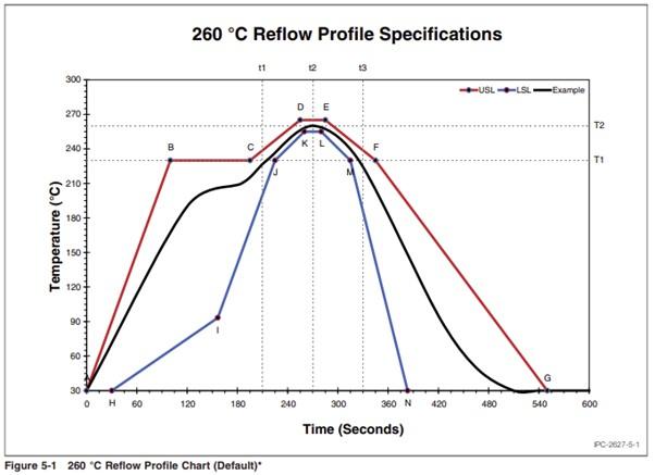
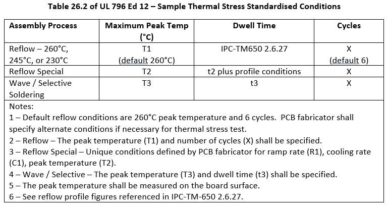
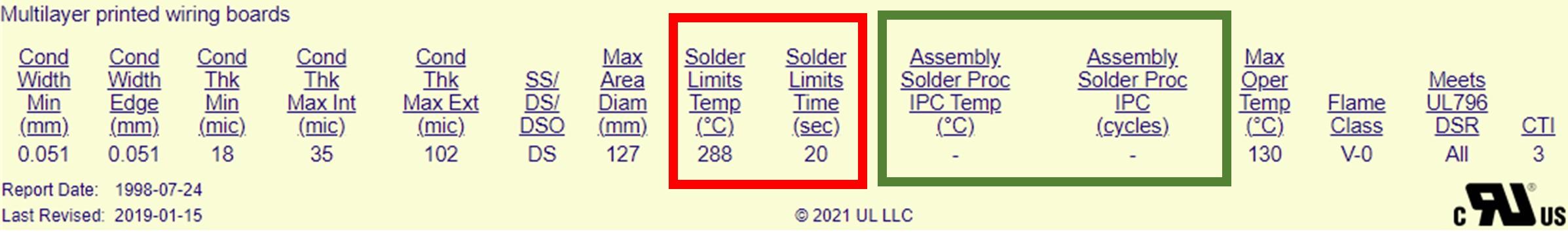
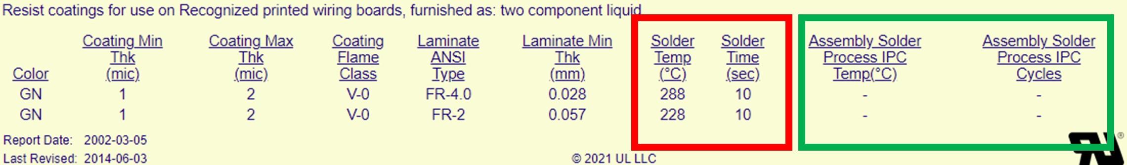
I think the first time I spoke to the industry on this topic was at the EIPC Winter conference in 2018. The rules had not yet been established of how a change should be implemented, but it was clear something had to be done about the Solder Limits parameter used as part of the UL PCB Recognition. I was still at UL at this time, and it had long been a personal bugbear of mine that most PCBs were Recognized with solder limits that were based on the old solder float test, hardly what you would call representative of the surface mount reflow profiles that the majority of PCBs are now exposed to during assembly. When I had previously worked for a tier-1 automotive electronics manufacturer, one of my tasks included establishing reflow profiles for our products so I knew that the commonly Recognized solder limits of 288°C for 20 seconds were nothing like the thermal excursions I would have put my boards through during assembly and that when we had to modify a reflow profile to increase the time and/or temperature, it could have an impact on the reliability of the PCB and resulting assembly. With UL Recognition, we are talking about SAFETY and if the modifications I could make to my reflow profile could influence the reliability of my product, what would moving from the solder float test to a more realistic reflow profile do for the safety evaluation of my PCB?! Nobody wants to skimp on safety, it’s one of those things that should be non-negotiable with a product, so things had to change and when we conduct the safety evaluation of the PCB we need to at least use solder limits that represent the actual soldering processes our PCBs are being exposed to in today’s assembly operations. So enough of my personal history with this topic and on to what solder limits are and what is going to be happening in the coming months and years. What is this Solder Limit parameter? Solder limits are a key parameter in the UL Recognition of a metal-clad material, solder resist, and Printed Circuit Board (PCB). They are used as part of the conditioning procedure for many of the tests conducted by UL, including flammability, bond strength and delamination. They were always meant to represent the soldering processes the PCB would be subject to during the component assembly operations. They should capture the temperature and time spent over 100°C or the Maximum Operating Temperature (MOT) of the PCB, whichever is greater, during the automated component soldering processes 1. But, for several reasons, most PCBs (and materials) are only Recognized with solder limits of a single time and temperature, which are based on the historical solder float test conditions (e.g. 288°C for 20seconds). As anyone who works in this industry knows, the old solder float test conditions are not representative of the actual soldering processes a PCB will be exposed to today. It is quite typical for a PCB to be exposed to at least two SMT reflow process steps plus maybe an additional wave and/or selective soldering operation, and possibly even rework.
Working with Industry
As can be seen, the default is now 6 cycles of the T260 profile but there are allowances for PCBs which will be soldered using a reflow profile that falls outside of the IPC-TM-650 2.6.27 criteria or that will be subject to only Wave or Selective soldering processes. This should help the PCB manufacturer to select the solder limits for their Recognition more easily.
What does it mean to the PCB manufacturer?
This will impact materials that have a metal-clad Recognition, as solder limits are one of the parameters used to assess the materials in these categories. Testing would include bond strength and delamination, and flammability, the same as was required for the original Metal-clad Recognition (or flammability testing for Flame Only materials).
This will impact the solder resist manufacturers in much the same way as for the laminate manufacturers, as solder limits are one of the parameters used to assess the materials Recognized under the solder resist category. To upgrade existing solder limits, it will mean that flammability testing is required.
During the FUS inspection at the PCB assemblers and/or the end customer, the UL representative will check that the PCB being used in the product meets the requirements needed for the end product certification. This includes whether the solder limits are being exceeded. • Number of soldering steps does not exceed the number of soldering cycles the PCB has been Recognized with The UL representative will not be required to inspect all the intricacies of the actual reflow profile, just the two items detailed above, if the PCB has solder limits Recognized in combination with one of the IPC standardised reflow profiles. If a PCB has been Recognized in combination with any of the other options provided in Table 26.2 of UL 796 (summarised earlier) then a more detailed inspection may be needed. If the PCB is found to have been used outside of its Recognized solder limits, this invalidates the Recognition and, a worst case scenario is, the assembler could be prevented from using the boards without further testing taking place. Recommended next steps: 1 – An exception exists for hand soldering operations. PCBs that will only be subject to hand soldering do not need to comply with the solder limits. |
|
Section 5 |
PCB Solderability Assessment - During and Pre-Production Bob Willis Bobwillis.co.uk |
||||||
|
Bob Willis |
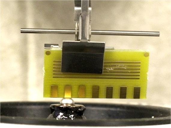
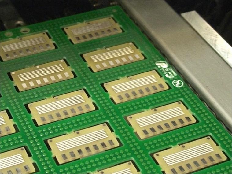
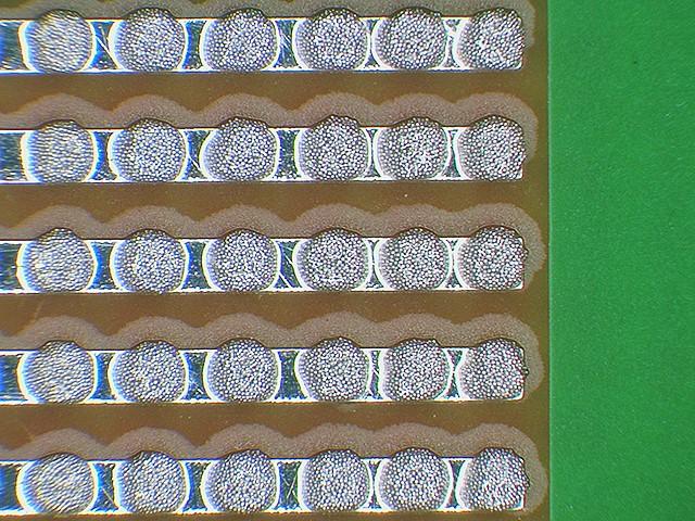
Solderability testing has become more common in the industry, particularly to assess printed board surface finishes during the transition to lead-free manufacture. The wetting balance is the standard method of test and provides the repeatability that other methods do not. The wetting balance is the more professional way of assessing the performance of printed boards finishes, but has not been used that extensively in the assembly or fabrication industry due to the cost of the system. During research and development, surface finish suppliers and solder material producers have used wetting balances to assess and demonstrate their products performance. In a recent study the author tested selected finishes in a live production process in Stockholm, Sweden. The production lines allow assessment of the changes in solderability that can take place as boards pass through one and two reflow processes. Also the effect of different hold times between soldering second side SMT or through hole can be assessed. Having a hold time between first and second soldering step can have a marked impact on copper OSP and tin surface finishes. This is less noticeable with gold or LF solder levelled boards. The production process was run at a major electronics exhibition in Sweden, called SSE (Swedish Electronics Exhibition). In addition we ran the test coupons with the solder paste spot test pattern. We have had many years of experience of using this shop floor assembly test and we have available all of the criteria, design files and results, for any potential user. 
Images above show the testing of PCB samples during production
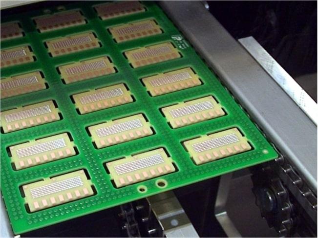
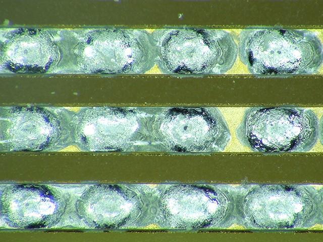
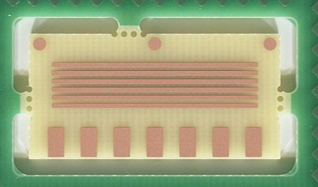
Images show test coupons passing through reflow soldering with alternative solder The tests often conducted in printed board manufacturing facilities, are well documented in international standards, but are not really representative of the requirements of modern assembly. Rotary dip and solder float solderability test methods are both used by the printed board industry, but are very limited and basically the same as the dip and inspect test, still used by surface mount component producers. It is very difficult to demonstrate the subtle changes which take place on boards and components as they are subjected to multiple heating operations during manufacture or assembly. When specifying new finishes for lead-free, the procedure to demonstrate and assess solderability must be established. The suppliers test criteria must be reviewed for effectiveness and suitability. The artificial ageing methods and parameters used should also be considered, so that confidence can be achieved in the supplier’s ability to control his process and the consistency of products supplied to the end user. A wetting balance can be used in two modes for testing printed board test coupons. Either using a solder bath, or the preferred method which is the solder globule test. In the case of the test coupons shown below, either individual test pads or oblong pads, shown on the bottom of the samples are tested with the globule method. Alternatively the seven pads could be tested simultaneously with a solder bath, which was the method used during the "First Lead Free Hands On Experience" organised by the author. This is not ideal as the results are more difficult to interpret due to the buoyancy of the samples.
Top left Ag (Silver) Top right Au (Gold/Nickel) Bottom left Sn (Tin) Bottom right Cu (Copper OSP) To provide repeatable results the wetting balance may be used to assess changes in solderability on test pads, audit panels or even pre-production boards. Test pads can typically be 2mm x 3.5mm (0.080” x 0.138”). Smaller pads can be used with smaller solder globules to better reflect what is used in the industry, however, alignment of the sample is then more demanding for the operator. The author has spent many hours doing testing of this type and can affirm that it is a demanding procedure. Camera alignment is a real benefit as test locations become smaller, it also provides greater repeatability of testing. With modern assembly processes the boards are often subjected to pre-baking, adhesive curing, wave soldering and cleaning. Each step will affect solderability to some degree. Furthermore the board may also have been subjected to a reflow soldering process for topside mounted components. In the case of double sided products, one or two high temperature reflow processes may also be experienced. The hold time between side one and side two and the use of reflow or wave soldering can be assessed by the wetting balance. The benefit of using air or nitrogen reflow can also be quantified. The impact of different levels of nitrogen on solderability performance can also be gauged to reduce costs. Other process stages that are known to affect solder finishes include board washing, adhesive curing and handling. In each case the test pads can be used to assess the impact of the previous process stages.
Examples of the solder paste spot test pattern before and after reflow soldering
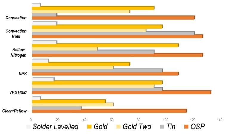
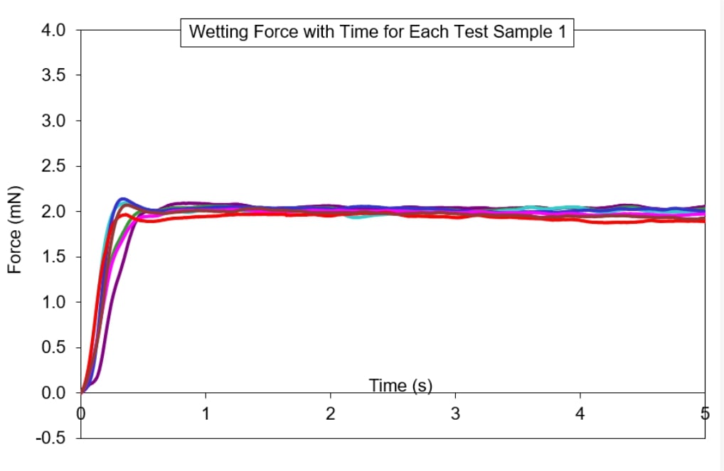
The results above show the changes in the wetting scores between finishes and after different assembly processes. The lower the numbers the better the solderability. We have normally found that the spot test results are inline with the wetting balance results. This has been demonstrated in other projects run at NPL (National Physical Laboratory) When a solder pellet is used for tests it is conducted at 235oC for tin/lead using a 200-250mg solder globule on a 2mm globule block with an immersion depth of 0.1mm. The immersion speed for the tests are typically 1mm/s with a dwell time of five seconds. In the case of lead-free, a higher temperature is used. A further benefit of the globule approach is the alloy used for the test can be the same as used in the assembly process. It has been highlighted many times the difference in wetting found between tin/lead and lead-free materials. The 200-250mg globule may be used on each pad to be tested without contacting the adjacent pad. Due to the size of the pad under test a new pellet is applied to the block after each test. This is due to the amount of solder removed on each test site. It is also necessary to remove the occasional solder spike from the pads to avoid them touching the globule block, affecting the next test result. Spikes can be caused by poor solderability but often by the cooling effect of the board and its mass. The tests can be conducted using both pure rosin and activated rosin flux to assist repeatability of assessment. In some situations with high mass test samples, separate pre-heating is possible Wetting Balance Solderability Testing Experience Although the solder spot test pattern has been used for many years the wetting balance is the standard industry test method and has been developed over the years for PCB finish assessment. Sample boards from the "Experience" previously subjected to one or two reflow cycles were tested 10 days after the first reflow by Gen3 Systems. The following graphs show the changes in solderability after one reflow operation; the results are exaggerated due to the hold time prior to testing. It is well known that some alternative surface finishes do not hold up to one reflow cycle followed by an extended hold time before the second soldering operation. This is a critical issue when selecting surface finishes. Some companies build their products or contract out the assembly and only complete the final assembly when orders are received. This situation is often not considered during the evaluation phase. Test conditions used on the wetting balance for the Sweden production line Solderability testing conducted with 200mg SAC pellet
The images above show a test panel and a close up of an individual test coupon
The selective wetting results shown below illustrate the results at different stages of assembly. A full copy of the presentation results is available from the author
Using these different techniques assembly companies and printed board manufacturers can use the wetting balance to guarantee the solderability of boards and components in their drive for zero defect manufacture. Both tests have often been used by the author for material evaluations, the impact on assembly process stages, the change in flux activity and supplier audits. They are also useful techniques as part of product development or to provide customers with technical support. Use of this test method eliminates the arguments which often arise when the soldering quality does not provide the expected soldering yields in production. |
||||||
| Go back to Contents |
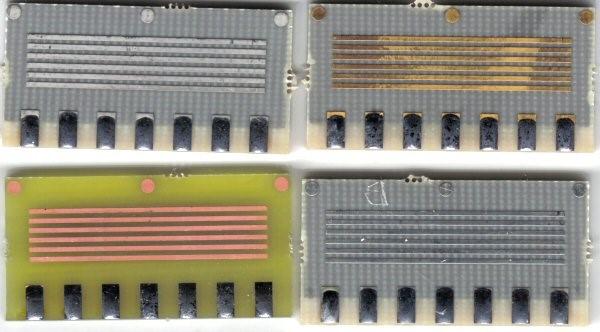 Top left Sn (Tin) Top right Au (Gold/Nickel) Bottom left Cu (Copper OSP) Bottom right Ag (Silver)
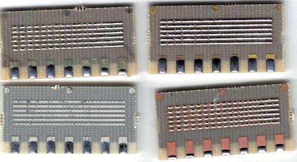
 Pre-test reference samples taken for each finish
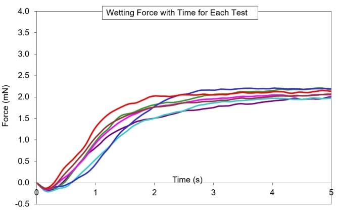 Post process exposure showing delay in wetting
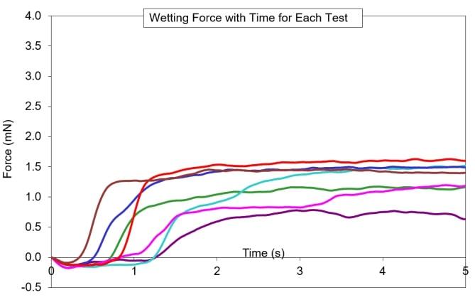 Variability in wetting forces after process exposure
|
Section 6 |
Jiva Soluboard Update Jack Herring |
|
Jack Herring |
Jiva has developed a fully recyclable and biodegradable PCB substrate – Soluboard®. On a global scale, 54 million tonnes of Waste Electrical and Electronic Equipment (WEEE) is produced every year. This number shows no sign of decreasing and the UK alone contributes an average of 2 million tonnes to the fastest growing waste stream every year. Printed Circuit Boards or ‘PCBs’ contribute significantly to this waste. PCBs are currently constructed from epoxy resin and fibreglass. The only commercial method of processing waste PCBs involves shredding and incinerating them to extract precious metals. This inefficient process is very energy intensive and results in a substantial loss of value of any precious metals recovered. The primary ingredient in Soluboard® is a natural fibre with a much smaller carbon footprint than glass-based fibres. The multilayer bio-composite structure of Soluboard® will meet the mechanical and electrical requirements of most sectors within the electronics industry. Soluboard® is created using natural fibres combined with a number of other biodegradable ingredients that once immersed in warm water, will cause the layers of the composite material to delaminate. This allows the natural fibres to be composted, the remaining solution to be disposed of using standard domestic waste water systems and the electronic components to be removed for re-processing.
Negating the need to incinerate material is accompanied by a significant reduction in carbon that is released into the atmosphere. It has been estimated that 10.5kg of carbon per square metre of Soluboard® PCB would be saved in comparison to existing technologies – this would suggest a 60% reduction in the PCB substrate supply chain. If Soluboard® was used in just 1% of European domestic appliances, 100 tonnes of plastic waste would be eradicated from the waste stream. Upon commercialisation, Soluboard® would be actively reducing the 215,000 tonnes of e-waste that London produces each year.
Printed electronics uses common printing equipment such as screen printing or inkjet printers to create electrical devices on various substrates. These processes deposit functional inks on to the substrate - functional inks are electrically active materials that have conductive properties. Printing processes are deal for prototyping. Whilst flexible substrates are more commonly used with printed electronics, the technology is also compatible with rigid PCB laminates - this includes Jiva's Soluboard®. With the support of one of our key UK-based partners, Printed Electronics Ltd (PEL), Jiva now has the ability to produce fully functioning Soluboard® prototype PCBs using printed electronics. One example of the prototypes that Jiva and PEL are able to produce is a single-sided variant of the open-source Arduino, a microcontroller commonly used throughout the maker community.
Jiva’s Soluboard® is also available as a Copper Clad Laminate (CCL) for use in typical PCB fab-houses. Jiva has optimised the material to be compatible with drilling, routing, curing and even water-based etching processes. By following Jiva’s processing guidelines, Soluboard® customers can fabricate PCBs comparable to the FR-4 alternative. Jiva’s Soluboard® will be available for purchase as CCL as well as in its raw form for printed electronics applications. |
| Go back to Contents |
|
Section 7 |
ICT Webinar Review: Pete Starkey, I-Connect007 |
 |
Since its establishment in 1974, the Institute of Circuit Technology has continued to keep the UK's PCB technologists and engineers up-to-speed with developments in the industry. While operations are progressing back toward normality, it may be some time before its seminars are re-established as physical gatherings that combine learning with informal opportunities to network. But the Institute continues to deliver first-class on-line events. This year's ICT Autumn Webinar on September 7 presented papers by leading experts on high-voltage testing and advanced antenna materials. It was introduced and moderated by ICT Chair Emma Hudson. |
|
Martin Wickham |
High-Voltage, Partial-Discharge Testing of PCBs and Coatings Martin Wickham Martin Wickham, senior research scientist at the National Physical Laboratory, gave an insight into current work on high-voltage partial-discharge testing of PCBs and coatings. There was an industry trend toward higher operating voltages, particularly in automotive and power electronics applications. Ceramic-based devices had been the traditional choice for power modules, although these were associated with heavy weight and high cost. The potential benefits offered by organic printed circuit substrates tended to be limited by electrical discharge effects. Whereas full electrical discharge was a relatively well-known phenomenon, typically associated with catastrophic failure, partial discharge was not as clearly understood, and was currently being investigated. What was the nature of these effects? Wickham began by describing full electrical discharge in terms of the breakdown that occurred when a strong electric field pulled valence electrons from their atoms, rendering them mobile, and he gave comparative figures for air and PTFE as examples of low and high breakdown field strength. By comparison, partial discharge occurred as a “spark” in the insulation between two conductors at a point where the electric field exceeded the local dielectric breakdown strength. This could occur multiple times and progressively reduce the breakdown strength of the insulation. Paschen's Law defined breakdown voltage in terms of the product of gas pressure and the distance between electrodes, and had particular significance in aerospace applications because of the variation of pressure with altitude. Wickham explained that partial discharge occurred when the rate of change of voltage was highest, and that higher frequencies increased the likelihood, along with higher temperatures and lower pressures, although several complex interactions were also involved when factors like voltage waveform, humidity and contamination were considered. Collaborative projects at National Physical Laboratory had evaluated a range of antennas for detecting partial discharge at ambient and lower pressures. The range included circular antennas, PCB-based and commercial off-the-shelf, long and short monopoles, and twisted insulated-wire pairs. The twisted pair had been chosen as the test vehicle, and the current work-plan was to study the effects of frequency, overvoltage, atmospheric pressure, and waveform. Wickham described the test equipment, remarking that health and safety had been a primary concern since it was capable of operating at voltages up to 5kV. The electrical system included a power supply unit, waveform generator, and high-voltage amplifier. A vacuum chamber enabled pressure to be reduced to 0.1 bar, and insulation resistance was simultaneously monitored as the test materials progressively aged. He showed examples of partial discharge test results on a twisted wire pair, using a 500Hz sinusoidal signal. Partial discharge spikes could be observed twice per cycle at an inception voltage of 3.8kV peak-to-peak, equivalent to an RMS voltage of 1.343kV. The extinction voltage was 3.2kV peak-to-peak and the sample had an insulation resistance of about 50GΩ. After aging the sample for 8.5 hours with a sinusoidal 1kHz waveform at a voltage set to 3.8kV to support continuous partial discharge, insulation resistance had fallen to less than 10MΩ. The current work plan was to study the effects of frequency, overvoltage, atmospheric pressure, and waveform—sinusoidal or square-wave. Coatings were being studied in a separate experiment, observing surface insulation resistance, dielectric withstanding voltage and dielectric breakdown on B24-type test coupons with commercially available conformal coatings, aged in a normal 50Vdc SIR test in an 85°C/85%RH environment. No degradation in surface insulation resistance had been observed during a 1000-hour test. Neither did the samples show any disruptive electrical discharge during a one-minute dielectric withstanding voltage test at 1500Vac. Leakage current was less than 10 microamps, which complied with IPC and ASTM specifications. When a 3.6kV peak-to-peak 50Hz square wave signal was applied, some partial discharge could be observed. In another example, a 1kHz sinusoidal signal at 4.22kV peak-to-peak resulted in dramatic drop in insulation resistance and failure after only five minutes. Further work was planned using a test coupon designed by Manchester University, and three suppliers had agreed to provide coating samples for evaluation. National Physical Laboratory was seeking collaboration from PCB fabricators to advise on representative track-and-gap dimensions and to produce coupons on a broader range of materials. Wickham stressed the significance of the work, since the increasing uptake of high voltage electronics would inevitably result in more damage by partial discharge in PCBs, even if the power module designers continued to specify ceramic substrates. |
|
Ken Klapproth |
The ‘Last Mile’ Challenge Ken Klapproth “Despite decades of technological evolution, connectivity remains a challenge for 5G,” said Ken Klapproth, chief marketing officer at CHASM Advanced Materials, in his opening statement, then continued to describe how a new category of advanced materials enabled overcoming the “last mile” challenge. Reviewing the history of the mobile phone through its successive generations over the past 40 years, from early analogue systems to present-day emerging 5G, it is an undeniable fact that calls still drop out. Despite its lower latency and its enormous increase in traffic capacity and network efficiency when compared with its 4G antecedent, connectivity remains a challenge with 5G since its operating wavelengths have comparatively limited range and signals that could be interrupted by natural surroundings and physical obstructions. “With many technological advances, it seems like it’s always one step forward and two steps back,” he said. “Sometimes as engineers we make our own mess.” Klapproth envisages an explosion of antennas: it is forecast that the worldwide rollout out of 5G, smart and internet-of-things will necessitate tens of billions over the next four or five years as all this unified connectivity will rely on an antenna to connect each device to the network. Even with the benefit of advanced antenna technologies, most connections will need to be line-of-sight to permit high data rates and minimise interference. There will be 5G cell towers and antennas everywhere, on every lamppost and traffic light. And the interiors of factories and office buildings will be smothered with wireless access points. How could those antennas be hidden, or placed in inconspicuous locations, while remaining close to people? And what about autonomous vehicles and advanced vehicle safety systems? Window glass has been recognised as a potential solution, in buildings, machine enclosures and vehicles: generally well-positioned and with adequate area, but antennas needed to be transparent for both practical and aesthetic reasons. Klapproth discussed the properties of new materials that could resolve design challenges and fulfil the requirement. He explained that antennas were typically fabricated using strongly conductive metals such as silver, copper, or aluminium, with electricity being conducted in the form of radio waves. Skin effect, the tendency of an alternating current to be distributed within a conductor such that the current density was highest near the surface, increased with increasing frequency. At radio frequencies the current effectively flowed only on the surface of the conductive material, so that high frequency transmissions could be supported by very thin materials. Few available materials were both conductive and transparent. Indium tin oxide had been dominant in the market, but imaging to form conductive patterns was complicated and expensive. A new category of materials known as nanotube hybrids provided the required conductivity and the desired transparency, and could be imaged by simple screen printing rather than laser ablation. Nanotube hybrids were enablers for transparent antennas; Klapproth reviewed their composition and structure. His high-magnification illustration showed a random array of metallic rods which were silver nanowires, embedded in a spaghetti-like matrix of single-wall carbon nanotubes. Conductivity could be increased by adding more silver nanowires or increasing their diameter, although this would also result in reducing transparency. The hybrid material overcame the traditional trade-off between conductivity and transparency, taking advantage of the unique properties of nanotubes: self-assembling and rendering the non-conductive areas between the nanowires conductive, as well as bonding the wires together, supporting applications such as bending or thermoforming. Even if the conductive rods were to be broken, there was sufficient conductive redundancy in the nanotubes to enable the signal to continue to be transmitted. These materials were more conductive and more transparent than any of their commercial alternatives. How to make connection to the transparent conductive film? Standard metal-mesh and silver nanowire films required some sort of over-coating for environmental protection, although this effectively isolated the conductive layer and needed to be etched, mechanically abraded or laser ablated in order to make connection. By comparison, in nanotube hybrids the carbon was environmentally stable and protective against moisture as well as being capable of making external electrical connections. Klapproth showed an example of an antenna circuit fabricated by simple screen printing of a nanotube ink on to a metal-mesh film, the ink doubling as an etch resist, then etching away the exposed metal mesh. He referred to real-world projects and applications. His example of a monopole Bluetooth antenna demonstrated that carbon nanotube hybrid out-performed copper in gain and frequency response. |
|
Emma Hudson moderated a productive question and answer session before bringing another successful ICT webinar to a close, thanking all who had participated and acknowledging the proficient organisation of the event by technical director Bill Wilkie. She was optimistic that a physical seminar would be possible before the end of the year. |
|
 |
Published by kind permission of Pete Starkey, I-Connect007 The Webinar can be viewed on the ICT You Tube Channel here |
| Go back to Contents |


|
Section 8 |
Directors ReportBill Wilkie, ICT |
|
Bill Wilkie |
Interconnection Systems, but not Limited It is often said that we know our ‘customers’ and they know us and this maxim has been shown to be valid, just recently. We’ve never believed in the shotgun principle in recruiting new members but have always relied on targeting senior people and those who know us in the sure knowledge that they will pass on requests to a wide range of friends and colleagues. We do have a presence on social media, mainly Linkedin, but even with 50 searches a week on our web page and 60 – 100 contacts (emails) a month, none are of any benefit to the Institute – shotgun targeting at its best! We also have an instance of targeted mail to members which resulted in Jeremy Rygate of Holders Technology enquiring if colleagues were able to get a copy of the Journal, with the result that we now have two new Members. Similarly, the many members we have in Fineline VAR prompted Steve Brockhill to apply for Membership. We get new Members because our various systems interconnect but not connected in any way to the behemoth of the ‘80’s and 90’s in South Shields! |
| Go back to Contents |
|
Section 9 |
PCB Fabricators Group - a Benefit to all who Fabricate PCB’s in the UK. |
|
The next meeting of the Fabricators Group is due the week commening 4th October, An update will be pulished in the next issue of the Journal. |
|
Section 10 |
Industry News |
|
Company |
Title |
|
Adeon |
ACB Group Invests in State of the Art Flying Probe Test System from ATG-LM The ACB group is one of Europe’s largest independent manufacturers of highest technology printed circuit boards. The group consists of manufacturing facilities at Dendermonde (Belgium), Atlantec and Cibel (France)
|
|
Electra |
Productronica 2021 - November 16–19, 2021 Messe München In these uncertain times when travel restriction are still upon us a question needs to be asked. , do we attend or do we not? I for one am glad to say that Electra has made the decision to really push to get back to normality and decided to attend Productronica 2021. The decision was based on conversations with customers and the desire to reconnect with our customers face to face, not to mention the fact that Electra has some exciting new developments in inkjet Soldermask, ident and etch resist. Although Electra will be taking a smaller contingent than normal, we feel this will still give our customers the chance to discuss Electra’s offerings on Inkjet, DI Soldermask and PCB related materials. Electra hope to see a good presence from our UK and European base and will be happy to invite you in to our booth for discussion on any subject PCB or other. Shaun Tibbles |
|
Merlin |
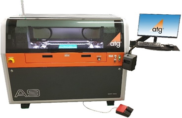
Merlin invests in testing automation, reducing test times and driving improved efficiencies. The exciting new addition to the Merlin test department is a fully automated ATG A5 bare board testing machine.The printed circuit board industry has ever demanding designs with reduced features and tightly packed circuitry. The ATG A5 is an 8 head machine with soft touch probes testing down to 50um features to meet the requirements of latest PCB designs. Read more.... |
|
Ventec |
Distribution of Taiyo Products We are pleased to announce that Ventec will be taking over the distribution of Taiyo products in mainland Europe, the UK and Ireland. Effective October 1, 2021, customers in Europe will immediately benefit from the supply chain partnership with Ventec, as it will grant greater and faster access to Taiyo product inventories which will be stocked and fulfilled from Ventec’s distribution hubs in Germany and the United Kingdom. As a leading provider of specialty dielectric inks and via filling inks for use with microvia and build-up technologies, legend inks, dielectric and conductive ink products for the solar, lighting & display markets as well as thermal-cure and UV-cure solder masks, Taiyo America will continue to provide sales and technical support to its direct customers, with Ventec providing supply chain fulfillment and invoicing services. For all other customers, Ventec will offer sales, technical, supply chain / distribution support. The agreement also opens up the opportunity for Ventec to offer Taiyo’s innovative range of specialty inks and solder masks for printed circuit boards to Ventec’s own strong and varied customer base in Europe from industries including medical, aerospace, consumer electronics and automotive. Read more.... |
| Go back to Contents |
|
Section 11 |
Members News |
|
Mike Fisher |
Mike Fisher, Industry stalwart and joint founder of Express Circuits with Ian Chalmers passed away last month from a heart attack at the age of 78. Mike was Production Manager at Plessey Ilford in the mid 70's and I remember being told that that the 50 high spirited women who ran the assembly lines could be a bit of a handful on a Monday morning. He joined what was Thiokol Dynachem in the mid to late 70's, at the same time as Pete Starkey, who had followed Ian Chalmers in the same position. Mike recruited me to Dynachem in '79 and like the others found Mike extremely helpful as you were finding your feet. He didn't suffer fools at all, but was an elder statesmen to all us young reps. He left Dynachem to join with Brian Saville in running Trulon Circuits and then joined with Ian at Express until his retirement. Mike will be sadly missed as a straight, uncompromising, colleague, with a big heart, who was one of the pre-eminent fabrication people of our era. Photo supplied by Mike's wife Antoinette Bill Wilkie Condolences: |
|
Exception PCB |
Mark Booth cycles 170 miles in three days and raises over £3300 for The British Heart Foundation |
| Go back to Contents |


|
Section 12 |
Membership News |
|||
|
12.1 |
Membership Update
|
|||
|
Bill Wilkie
|
NEW MEMBERS SUMMARY July-Sept 2021 |
|||
| Membership No | Name | Company | ||
| Fellows | ||||
|
10167 Reinstated |
Victoria Blaisdell | Holders Technology | ||
| Members | ||||
| 10549 | Steve Brockhill | Fineline VAR | ||
| 10560 | Alan Henderson | Holders Technology | ||
| Associates | ||||
| Go back to Contents | ||||
|
Section 13 |
Corporate Members of The Institute of Circuit Technology |
|
| Adeon Technologies BV | Weidehek 26,A1 4824 AS Breda,The Netherlands | www.adeon.nl |
| Atotech UK Ltd. | William Street, West Bromwich. B70 0BE | www.atotech.com |
| CCE Europe | Wharton Ind. Est., Nat Lane, Winsford, CW7 3BS | www.ccee.co.uk |
| ECS Circuits Ltd. | Unit B7, Centrepoint Business Park, Oak Road, Dublin 12, Ireland | www.ecscircuits.com |
| Electra Polymers Ltd. | Roughway Mill, Dunks Green, Tonbridge, TN11 9SG | www.electrapolymers.com |
| The Eurotech Group | Salterton Industrial Estate, Salterton Road, Exmouth EX8 4RZ | www.eurotech-group.co.uk |
| Exception PCB Solutions | Ashchurch Business Centre, Alexandra Way, Tewkesbury, Gloucestershire. GL20 8NB | www.exceptionpcb.com/ |
| Merlin PCB Group | Hawarden Industrial Park, Manor Ln, Deeside, Flintshire, North Wales, CH5 3QZ | www.merlinpcbgroup.com |
| Faraday Printed Circuits Ltd | 15-19 Faraday Close, Pattinson North Ind. Est., Washington. NE38 8QJ | www.faraday-circuits.co.uk |
| Graphic plc | Down End, Lords Meadow Ind. Est.,Crediton EX17 1HN | www.graphic.plc.uk |
| GSPK (TCL Group) | Knaresborough Technology Park, Manse Lane, Knaresborough HG5 8LF | www.gspkcircuits.ltd.uk |
| Amphenol Invotec Ltd | Hedging Lane, Dosthill, Tamworth B77 5HH | amphenol-invotec.com |
| HMGCC | Park Rd, Milton Keynes MK19 7BH | www.hmgcc.gov.uk |
| Holders Technology UK | Tweedbank Industrial Estate, Tweedbank, Galashiels TD1 3RS | ww2.holderstechnology.com |
| Minnitron Ltd | 20 Leigh Road, Haine Industrial Park, Ramsgate, Kent CT12 5EU | www.minnitron.co.uk |
| PMD (UK) Ltd. | Broad Lane,Broad Lane,Coventry CV5 7AY | www.pmdgroup.co.uk |
| Rainbow Technology Systems | 40 Kelvin Avenue, Hillington Park, Glasgow G52 4LT | www.rainbow-technology.com |
| Stevenage Circuits Ltd | Caxton Way, Stevenage. SG1 2DF | www.stevenagecircuits.co.uk |
| Sun Chemical | Norton Hill, Midsomer Norton, Bath | www.sunchemical.com |
| Teledyne Labtech | Broadaxe Business Park, Presteigne LD8 2UH | www.teledynelabtech.com |
| Ventec Europe | 1 Trojan Business Centre, Tachbrook Park Estate, Leamington Spa CV34 6RH | www.ventec-europe.com |
| Zot Engineering Ltd | Inveresk Industrial Park Musselburgh, B19EH21 7UQ | www.zot.co.uk |
| Go back to Contents |
|
Section 14 |
ICT Council Members |
|
Council Members |
Emma Hudson (Chair), Andy Cobley (Past Chairman), Steve Payne (Deputy Chairman), Chris Wall (Treasurer), William Wilkie (Technical Director, Membership & Events), Richard Wood-Roe (Web Site), Lynn Houghton (Hon Editor), Matthew Beadell, Martin Goosey, Maurice Hubert, Lawson Lightfoot, Peter Starkey, Francesca Stern and Bob Willis, |
|
Section 15 |
Editors Notes The ICT Journal |
|
Lynn Houghton |
Instructions / Hints for Contributors 1. As it is a digital format the length is not an issue. Short is better than none at all! 2. Article can be a paper or a text version of a seminar or company presentation. Please include data tables, graphs, or powerpoint slides.We can shrink them down to about quarter of a page. Obviously not just bullet points to speak from. 3. Photo's are welcome. 4. We would not need source cross references 5. Title of presentation - Of course! Date, Job title of Author and Company represented. 6. An introductory summary of about 150 words would give the reader a flavour of what it's all about. 7. Style - we don't want out and out advertising but we do recognise that the speaker has a specialism in the product or process that will include some trade promotion. Sometimes it will be a unique process or equipment so trade specific must be allowed. 8. Date and any info relating to where or if this article may have been published before. 9. We can accept virtually any format. Word, Powerpoint, publisher, PDF or Open Office equivalents. 10. Also, to make it easy, the author can provide a word file to go along with his original powerpoint presentation and I/we can merge it together and select the required images. 11. A photo of author or collaborators.
I really do look forward to receiving articles for publication. Lynn Houghton |