
Institute of Circuit Technology Darlington Seminar
18th November 2014
A long drive up to the North East of England on November 18th for the Institute of Circuit Technology annual Darlington Seminar, held on the site of the former World War II Royal Air Force Bomber Command Station, Middleton St. George, now Durham Tees Valley Airport. ICT Technical Director Bill Wilkie introduced and moderated a diverse and thought-provoking programme, acknowledging the generous support of Faraday Circuits.
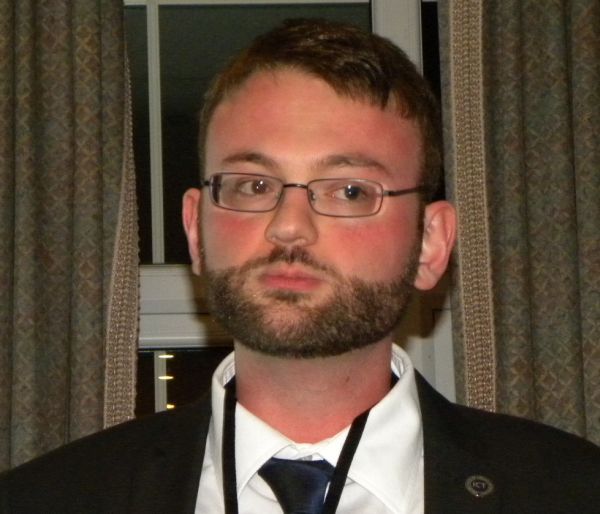 First to speak was Tom Jones from Merlin Circuit Technology, winner of the ICT “Best Young Person’s Technical Paper” award, with an extremely professional presentation on acoustic-assisted manufacturing techniques in the PCB industry.
Megasonic agitation, an acoustic technique working at much higher frequencies than ultrasonic agitation with less-damaging cavitation effects, had been successfully employed to enhance the filling of high-aspect-ratio blind micro-vias with electrodeposited copper. Jones described current work on the effects of megasonic agitation on the filling of high-aspect-ratio through vias. Some anomalies in copper thickness had been observed, with thin areas at certain positions along the length of the hole, and it was suspected that these were consequences of overtones and harmonics causing an acoustic standing wave within the hole. Hydrophone measurements of acoustic pressure corroborated the observed behaviour, positions of maximum pressure appearing to correlate with regions of reduced copper thickness. Modelling and simulation techniques were being used to investigate the impact on wave formation in response to changes to via size, acoustic impedance of PCB material and transducer position. Current-thieving by the transducer had caused variations in copper distribution on the PCB surface, including low current frosting and high current burning. The effects had been minimised by modifying the cell geometry, particularly moving the megasonic transducer further away from PCB, although this was a trade-off against the efficiency of agitation. In other process areas, indirect acoustic agitation with megasonics had been demonstrated to have the potential to improve pattern definition in developing and etching.
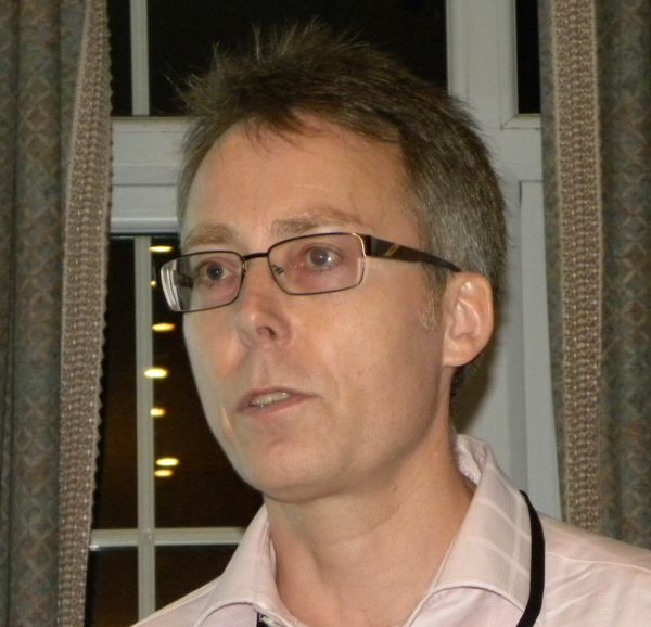
If only making circuits was easier! Tom Brown, Technical Manager of Holders Technology, whimsically suggested that every PCB manufacturer aspired to an 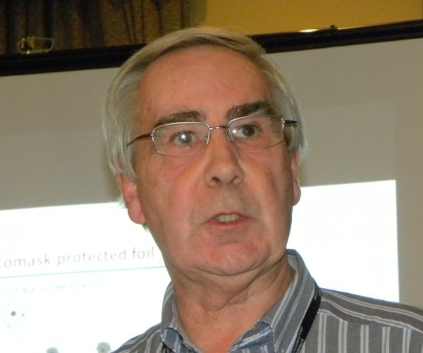 easier life – all he really wanted were higher manufacturing yield, lower cost of production and better product quality. But where to find them within the mix of materials, equipment, chemical processes, mechanical processes and people? Some solutions were high-tech, some were highly automated, but not all depended on a high level of investment and need not be complex – indeed in certain cases a solution could lie in making things simpler.
Brown took the multilayer layup process as his example to review and considered issues associated with the use of thin copper foils, speculating upon the possibilities of making thin copper foils easier to handle and less vulnerable to damage, and protecting them against particulate contamination. Was this too much to expect? In Brown’s view it was not a dream but a practical reality and the answer was to laminate the copper foil with a proprietary protective film at the roll stage, prior to panelising. The protective film supported and protected copper during foil handling and throughout the lamination process, and was simply peeled off at the breakdown stage. Benefits included the elimination of epoxy spots and a reduction in pits and dents due to airborne particulates or damaged separator plates. In his experience this protective film significantly improved handling of thinnest copper foils, speeded-up the lay-up process, allowed user the choice of steel or aluminium separator plates and was suitable for automated handling systems. As a potential further economy, traditionally-generous oversizes on foil could be reduced.
 Dr Andrew Cobley, Director of the Functional Materials Research Group at Coventry University gave a presentation entitled “Conductive Fabrics to Enable Wearable Electronics” describing a new Knowledge Transfer Partnership project, in which Coventry University were collaborating with the National Physical Laboratory.
There was an increasing demand for wearable technology from industry sectors such as medical and healthcare, sport and fitness, consumer electronics and defence. The world market for wearable e-textiles was projected to grow from approximately $300 million to $1.5 billion by 2020, and healthcare would remain the dominant sector.
Various methods were available to introduce electrical conductivity into a fabric: woven metal threads, metal-coated fibres, carbon fibres, printed or deposited conductive polymers and inks, or plasma deposition of metal. Disadvantages of current methods were the poor conductivity of non-metallic fibres, the limited bendability and stretchability of metallic fibres and difficulties in achieving selective conductivity. Washability of conductive fabrics was an essential requirement.
The approach being taken in this KTN project was to fully encapsulate fibres within the fabric with a coating of nano-silver particles, formed in-situ on a chemically functionalised textile material. This resulted in 100% encapsulation of fibres in a 20 nanometre silver coating with excellent adhesion, flexibility and wash-resistance, although conductivity was limited but could be improved by electroless copper plating and applying immersion silver as a final finish. The process had been successfully demonstrated on a wide range of natural and synthetic textiles. The principles established presented opportunities for selective functionalisation by ink-jet or screen printing, such that useable electrical circuits could be created within the fabric.
Martin Cotton, Ventec’s Director of OEM Technology, can always be relied upon to deliver a dynamic and inspirational presentation. His down-to-earth discussion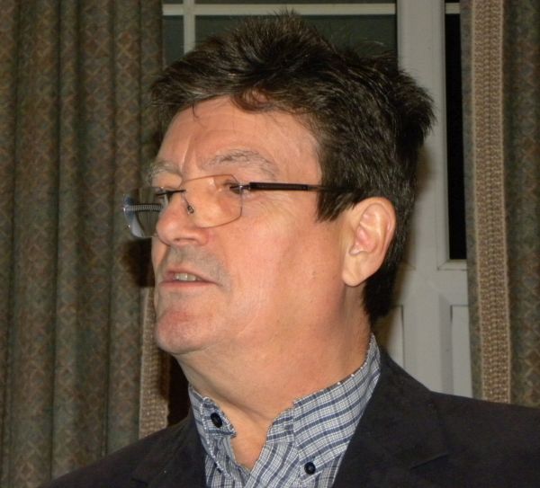 of practical design considerations for high speed PCBs was dedicated to the memory of the late Fred George Pochodnia, who had been a great motivator in the early days of his design career.
With the emphasis on “practical”, Cotton set out to build the basis of a design for a 36 layer backplane example, working at 10 Gigabits per Second data rate and 100 ohm impedance.
Initial questions to be answered were whether the data rate was for a single-channel differential pair or for a buss, buss speed being the total of all the channels in that buss. 100 ohm differential impedance used two tracks in harmony to keep losses to a minimum, and the geometry of those tracks and their positioning within the PCB build structure were critical to the realisation of a successful design, and the ability to manufacture it at a good yield. Setting-up the differential pairs in X, Y & Z axes began with material selection and consideration of dielectric constant and loss factor, then the creation of “cells” to define trace geometry, trace separation, pair separation, layer to layer separation, taking material properties into account – particularly dielectric constant – before carrying out impedance modelling. The completed “cell” was the essential foundation of the design. Once it was established, the designer could proceed to initial stack-up and trace mapping, and sample simulations on maximum trace lengths. Knowing the material and the build enabled cost estimates to be made. Only then would the actual layout proceed, with periodic checking simulations to ensure acceptable signal integrity.
In Cotton’s example, 36 layers were required to realise the design, but post-layout simulation revealed signal integrity issues with 90 differential pairs of the 2000 contained in the layout. The designer was then faced with a dilemma: to fix these by reviewing them individually, which would take time, or to move them from within the 36 layers and add four additional layers, plus two power planes for reference, making a total of 42, which would increase unit cost and could complicate the mechanical design. Another option might be upgrade to a more expensive material with better Dk and Df values, although Cotton stressed that in principle the material supplier should always be consulted in the first instance, rather than too late in the design process.
“Design once, make many times” was his message, “take the time to create what you set out to do”, adding that although CAD and simulation systems were very powerful tools the actual designing was done “up here” – pointing at his head!
 A long drive for some, but well worth the journey – the Darlington Seminar was another very successful event in the ICT calendar, combining technical enlightenment with a great networking opportunity for the many members who attended.
Pete Starkey, I-Connect007, November 2014