Institute of Circuit Technology Evening Seminar
Darlington, UK, 3rd November 2009
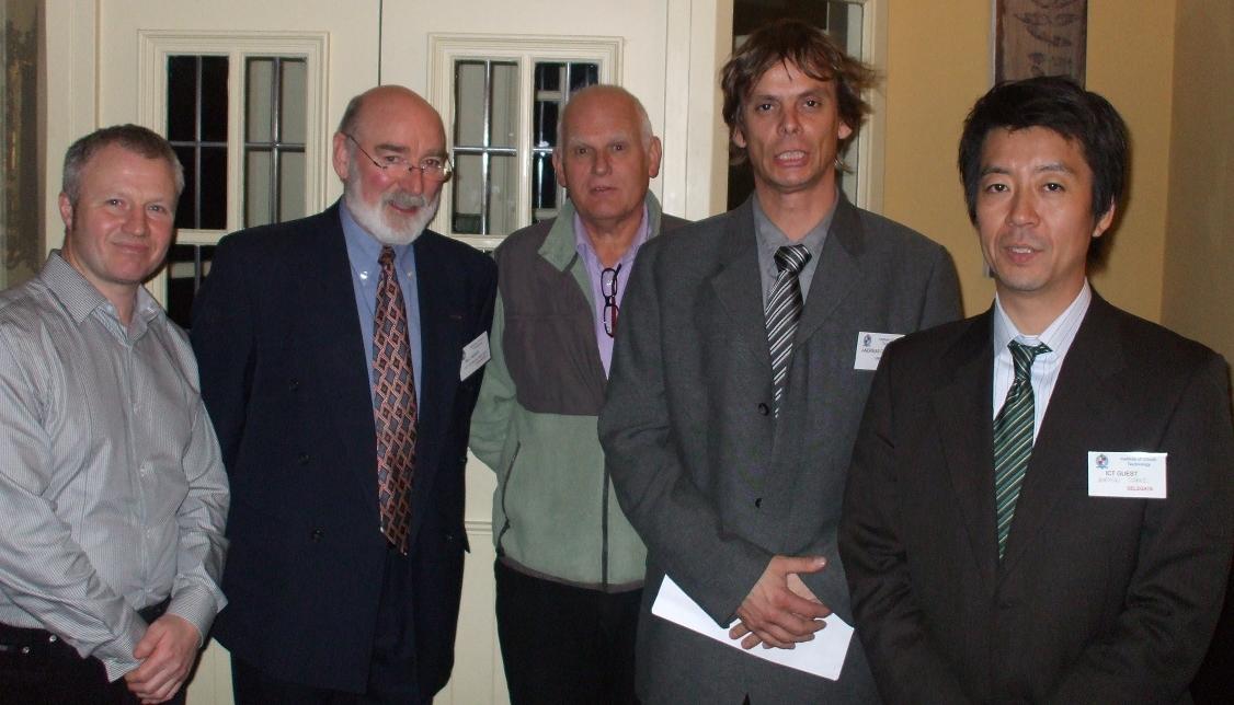
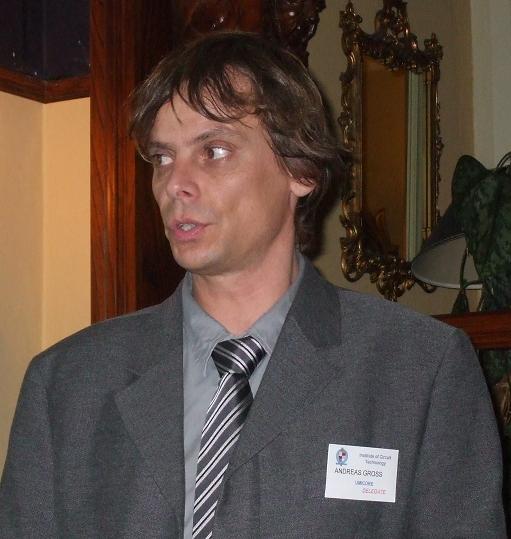 Our first speaker was Andreas Gross from Umicore Galvanotechnic in Germany, with a presentation on multifunctional electroless nickel-palladium-gold finishes for soldering and wire-bonding applications. Comparing alternative processes based on either immersion palladium or electroless palladium as the barrier layer between nickel and gold, he demonstrated that even a very thin palladium layer was effective in maintaining solderability after ageing by preventing nickel diffusion to the surface.
Because of its neutral operating pH, electroless palladium chemistry was less corrosive of the nickel interface than its acidic immersion counterpart during the deposition process. However, except in conditions of extreme thermal stress, electroless nickel immersion palladium immersion gold was a cost-effective and easy-to-operate multifunctional finish which had been customer-approved for mass production in Europe.
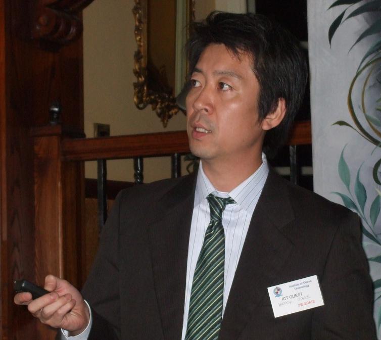 Examining in detail the technology of the electroless palladium process, Hiroshi Otake from Uyemura in Japan described an innovation which had overcome some limitations of traditional chemistry and offered significant improvements in uniformity of deposition rate, bath stability and adhesion of palladium to nickel. Uyemura had developed an additive which stabilised the palladium chelate and substantially reduced the decline of deposition rate with time. Bath stability was improved, especially at extreme conditions of bath loading. A notable characteristic of the modified chemistry was its ability to promote good adhesion of the palladium deposit even if the electroless nickel surface had deliberately been allowed to oxidise between process stages.
 George Wheadon, European technical service specialist for Park Electrochemical, gave the first of the two laminate presentations, introducing a newly developed low-loss material, branded Mercurywave 9350, which offered a cost-effective alternative to PTFE for radio frequency and microwave applications. Using fine-weave E-glass fabric and a 66% ratio of oxide-filled resin, loss tangent had been reduced to .004 at a dielectric constant of 3.5. No special facilities were required to process and fabricate the material. Dielectric characteristics were stable over a wide range of frequency, temperature and humidity and the material exhibited remarkable thermal properties – glass transition temperature above 200degC, very low coefficient of Z-axis thermal expansion and no delamination after 15 reflow cycles. The material was suitable for applications in base station equipment, automotive, satellite communications, military, and broadband antennae.
 Jim Francey, Technical Service Manager with Taconic, reviewed trends in RF-microwave and high-speed digital technologies, with particular reference to their effects on printed circuit board processing requirements. Although optical techniques would ultimately take over from copper to meet high frequency data rate demands, copper-based systems would continue to be used for gigabit-speed transmission in millimetre wavebands, such as those specified by the Federal Communications Commission for E-band and now adopted in Europe and the rest of the world. Printed circuits were preferred over low-temperature co-fired ceramics for reasons of assembly economics, lower tooling costs and a global supply base, but the issue would remain of managing signal losses: conductor loss and dielectric loss. Skin effects could be minimised by using highly conductive finishes for copper, and Francey believed that the recently introduced autocatalytic silver immersion gold ASIG, with silver thickness of 0.5 micron and gold thickness 0.05 micron offered the best option for both solderability and wire bonding. Wire bondability became significant where monolithic microwave integrated circuits were flush-mounted in cavities machined into the PCB surface to minimise induction losses by keeping bond wires as short as possible. From the fabricator’s standpoint, precision machining capability was essential. Similarly, imaging, etching and layer-to-layer registration became increasingly critical with increasing frequency. Low-loss materials were necessary in order to maintain signal integrity, and low-dielectric-constant laminates enabled reduced dielectric spacing for a given impedance. Signal integrity was degraded by woven glass, but the effect could be reduced by using finer weaves in combination with high resin content and fillers. Although thinner materials gave opportunities for tighter impedance control, this could be at the expense of compromising dimensional stability, requiring the printed circuit fabricator to maintain a high level of capability in dynamic process technologies such as laser direct imaging to compensate for material movement.
ICT Technical Director Bill Wilkie closed the formal proceedings, thanking the speakers for their contributions, the audience for their attention, and Holders Technology for supporting the event, and a buzz of informal technical discussion continued for a good while in the bar afterwards.
Pete Starkey
November 2009
