The Institute of Circuit Technology Tewkesbury Seminar, 1st March 2016
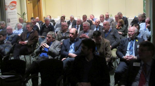
 The Annual General Meeting of the Institute of Circuit Technology was held at Puckrup Hall, near Tewkesbury in Gloucestershire, England, on 1st March 2016, and was followed by a well-attended evening seminar with presentations on a novel laser-induced deposition process, an analysis of the market for PCBs, and a review of three development projects in which the Institute had participated. The programme was introduced and moderated by ICT Technical Director Bill Wilkie.
Please note that copies of the presentations are available in the Members section
Could laser-induced forward transfer (LIFT) offer a novel deposition process for PCBs?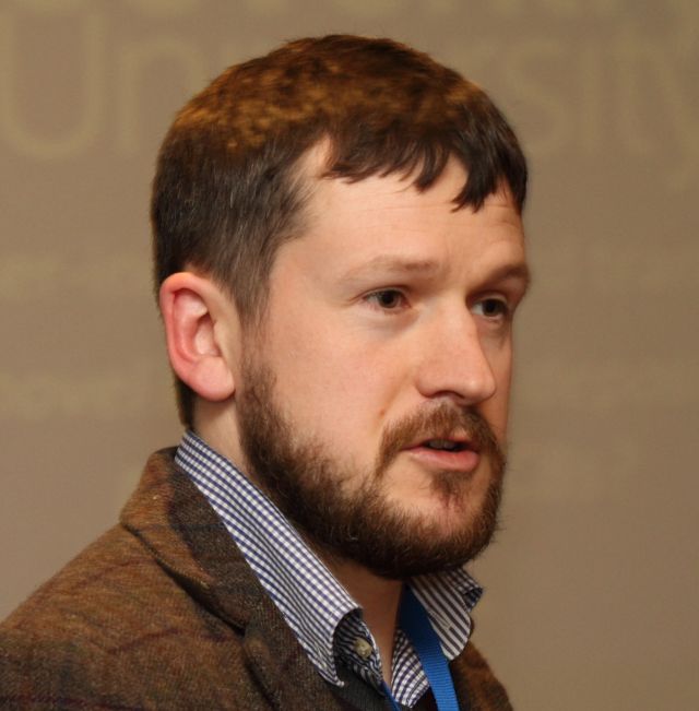 Dr James Shaw-Stewart, senior lecturer and researcher at Coventry University, gave an insight into the concept and applications of LIFT in transposing images from a donor substrate onto a receiver substrate. The transferred material could be a solid metallic or non-metallic film, or a liquid nano-ink, coated onto a sacrificial photosensitive layer on a transparent substrate. Ablation of the photosensitive layer by a laser caused transfer material to be propelled forward as “flyers”, and deposited on the receiver, placed a short distance away. A video illustration of an early example showed an 80 nanometre aluminium layer on a 350 nanometre photosensitive layer being successfully transferred across a 1 millimetre gap at a laser intensity of 270 milliJoules per cm2 and the efficiency of transfer increased as pressure was reduced from atmospheric. A further example demonstrated how a pulsed laser could be combined with a video image source to transfer a donor nano-ink to a substrate on an X-Y platform. The laser energy required to drive the transfer was significantly dependent on the viscosity of the ink.
LIFT techniques had been successfully used to build several different types of organic semiconductors, sensors and capacitors, and as a means of creating micro-bumps on flip-chip packages. The US Naval Research Laboratories had demonstrated the capability to laser-print metals to form microbridges and microcantilevers. More recently, extreme-aspect-ratio copper structures had been deposited from a solid copper donor. Dr Shaw-Stewart’s description prompted a question from the floor about the possibility of applying LIFT techniques to the repair of open circuits on PCBs and it was acknowledged that this was a topic worthy of investigation.
Dr Shaw-Stewart concluded his presentation with “something a bit different” - a discussion of what could be accomplished by a technique known as scanned mask imaging (SMI), a development in which he was collaborating, which achieved excimer-style beam uniformity with cost-effective solid-state lasers. The system used a scanning 355 nanometre laser, with optics to shape the beam and project it onto a static substrate through a static photomask, to structure interconnects as fine as 3 micron lines and spaces with 10 micron vias. Scanned mask imaging had the potential to bridge the 1 micron to 10 micron “technology gap” between silicon wafer and PCB design rules in advanced packaging applications.
 From imaging technology the attention turned to business forecasting. Market analyst and ICT council member Francesca Stern presented an outlook on the global PCB and electronics industry, beginning with an overview of trends in world electronics equipment production. Overall value in 2015 was about $1.5 trillion, almost unchanged from 2014, and distributed geographically: Asia 53%, North America 19%, Europe 15%, Japan 3%, Rest of World 10%. The forecast for 2016 was for a slight overall increase to $1.6 trillion.
Looking specifically at PCBs, world production in 2014 had been $60 billion, and this had declined about 3% in 2105 to an estimated $57.8 billion with slight growth in Europe and North America, no growth in Japan and a slight decline in South Korea and Taiwan. There had been a huge variation in the fortunes of the top twenty-five PCB fabricators in 2015, for example Fujikura showing as much as 46% growth whereas Daeduck’s figure was -22%, the overall average being 1.6% growth. Exchange rates could distort figures such that apparently positive growth measured in Asian domestic currencies could in fact be negative when converted to US dollars.
In terms of geographical distribution, of the $57.8 billion world PCB production total for 2015 China accounted for 46%, Europe 4%, and North America 5%. And the end market for PCBs was 45% in China, 10% in Europe and 8% in North America. The corresponding figures for 2016 were forecast to be $59 billion total, with production from China 46%, Europe 4% and North America 5%, supplying a market of which 46% in China, 10% in Europe and 8% in North America.
The outlook for the UK PCB industry was that the current downward trend would bottom-out mid-2016, and move into positive growth by the end of the year, peaking mid-2017 then cycle down again. European PCB production would follow a similar cycle, but with smaller peaks and troughs.
Back to technology developments, as Professor Martin Goosey took the floor with an update on ICT’s research and development projects, specifically the two 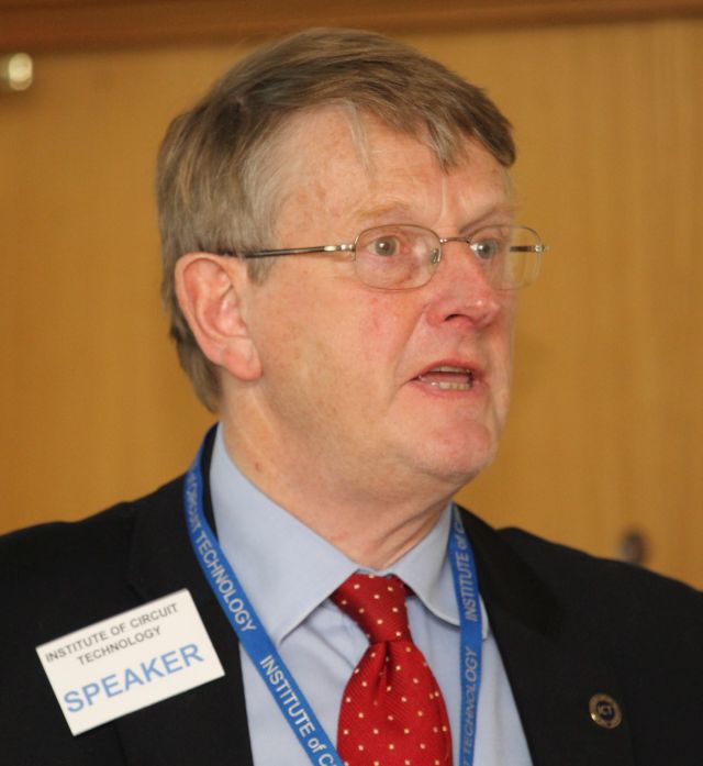 current Innovate-UK funded programmes in which the Institute was the dissemination partner, STOWURC and MACFEST. (The acronyms stand for Sustainable Treatment Of Waste Using Recycled Chitosans, and Manufacturing Advanced Coatings for Future Electronic Systems)
The two-year STOWURC project, which had developed new effluent treatment processes using materials derived from crab shells had just reached a satisfactory conclusion, and demonstrated how a natural waste product from one industry could be utilised to treat waste from another industry by removing and recovering trace metals from PCB and metal finishing process effluents. Background to the project was that the seafood industry produced large quantities of shellfish waste, which was becoming increasingly expensive to dispose of. The potential value of crab shells was that they contained a compound called chitin, which was capable of absorbing metals, and one gram of shell could potentially absorb up to 250 milligrams of copper. A typical PCB factory effluent could still contain several parts per million of copper after normal effluent treatment, which required to be reduced to lower levels to satisfy discharge regulations, generally by the use of ion-exchange resins. Crab shells offered a readily-available natural alternative, and the project partners had comprehensively investigated and optimised the physical, chemical and economic parameters required to achieve a practicable and cost-effective effluent treatment process, which was currently running successfully at 100 kg pilot-plant scale in a large PCB factory. An additional application of crab shell materials was as the active component in spill kits and static drag-out bags, to treat spills and localised effluent issues, and this had also been successfully demonstrated. Full details of the project and further information could be found on the website www.stowurc.co.uk .
The two-year MACFEST project had set out to utilise the properties of ionic liquids to produce solderable finishes with improved joint reliability, and had just passed its half-way point. New ionic-liquid-based nickel-palladium-gold systems were being investigated and
a process for the deposition of good quality palladium and gold coatings onto ‘aqueous’ electroless nickel has been developed. PCB test coupons were currently being prepared for evaluation, and would also be tested as part of a major SMART Group programme taking place over the coming few months. Potential benefits of coatings resulting from the MACFEST project would be a reduction of environmental impacts through the elimination of cyanide-based aqueous chemistries and a reduction in the amount of palladium consumed. The principal technical benefit would be the elimination of known reliability issues with nickel-palladium-gold finishes deposited from aqueous chemistry, particularly black pad effects, brittle joints and void formation. And the new coatings would meet the requirements of the industry and current IPC standards. Further information could be found on the website www.macfest-project.co.uk .
 Project Manager and Research Fellow at Coventry University, Narinder Bains gave the final presentation, on the optimisation of process conditions for the maskless electrochemical patterning of materials, with particular reference the university’s collaboration in the MESMOPROC project, co-funded by the EU Eco-Innovation initiative.
The concept of electrochemical ‘maskless’ selective metallisation of materials had been established and demonstrated in the Enface process, where instead of a plating resist image being applied photolithographically to each workpiece then stripped off after a single operation, the image was applied to the anode and effectively re-used many times. With the selectively masked anode placed close to the workpiece, and using a low-acid, low-metal electrolyte and good agitation, the pattern on the anode could be replicated in metal deposited on the workpiece, enabling selective metallisation of microscale devices, components and printed circuit boards. A limitation of the process had been the difficulty in maintaining the intensity and uniformity of solution agitation when scaling up the electrochemical reactor.
In the MESMOPROC project, low frequency ultrasound was introduced to the system to enable high efficiency, focused agitation. The team at Coventry, with many years’ experience of ultrasonics applications, had modified the reactor to incorporate ultrasonic transducers and had studied the general effects of ultrasound on the electrochemical deposition process. The team had then studied the effects of ultrasound on deposit quality in low metal, low acid copper electrolytes with commercial electroplating additives. It had been demonstrated that low or no acid electrolyte formulations, together with very narrow anode-cathode spacing gave the best image reproduction and good deposit quality, although low frequency ultrasound tended to increase additive consumption. The overall conclusion was that ultrasound increased the limiting current density and opened up the process window.
The MESMOPROC process had been demonstrated and validated at pilot scale in a PCB shop and a specialist plating shop, and offered enhanced efficiency through a shorter and simpler process using fewer materials and less energy, with reduced waste generation and CO2 emissions. Further information could be found on the website www.mesmoproc.eu.
In his closing comments, Bill Wilkie acknowledged the generosity of Exception PCB Solutions in supporting the event, and reported that the membership of the  Institute continued to increase, presently standing at over 350, with members drawn from over 100 companies. The seminar had once again brought together an enthusiastic group of industry professionals to further their technical knowledge and their awareness of business trends, and, equally importantly, to network with their peers.
I am grateful to Alun Morgan for allowing me to use his photographs
Pete Starkey
I-Connect007
March 2016