Institute of Circuit Technology Northern Seminar
Glasgow, 5th March 2013
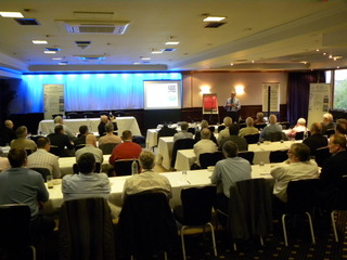
Not since the golden days of the Northern UK Circuit Group had such a gathering of the great and the good of the British printed circuit industry been seen north of the Scottish border. But the combined attractions of an excellent technical programme and a visit to Rainbow Technology Systems headquarters for a working demonstration of their innovative primary imaging process brought a capacity crowd to the Institute of Circuit Technology seminar in Glasgow on 5th March 2013. Welcoming delegates, ICT Technical Director Bill Wilkie commented that membership of the Institute continued to grow, and now exceeded 300.
 The first presentation of the seminar programme came from Stewart McCracken, Managing Director of MCS, with a description of a game-changing technique for microsection preparation. Many members of the audience, author included, had spent long hours at the laboratory bench, cutting, mounting, grinding, polishing, etching and examining sections of circuit boards or assemblies, conscious that critical details could be distorted or obscured as a consequence of the mechanical stresses involved.
McCracken was an expert in the application of Broad Ion Beam (BIB) machining to the microsectioning process. In principle, the technique involved masking-off the functional area of the sample and machining away the rest with a beam of energised ions in the form of an argon gas plasma. Material was removed at the atomic level, there was absolutely no mechanical damage – no smearing or deformation – and the true structure of the material was revealed. No potting resin was required, so an additional benefit was that, as well as the cut face of the cross-section, the adjacent surface could be examined, whether by optical or scanning electron microscopy.
He showed several examples of sections prepared by BIB, and clarity of detail and sharpness of edge definition were amazing. The technique allowed the critical examination of thin surface layers, such as immersion tin and immersion gold, and, when combined with scanning electron microscopy and energy-dispersive X-ray spectroscopy, the compositions of surface and sub-surface structures could be determined by superimposing elemental maps on the micrographs. In cross-sections of BGA joints, the copper-tin intermetallic phases were clearly seen and extremely fine Kirkendall voids could be readily detected in aged solder joints. BIB machining could be used to reveal otherwise hidden damage at interfaces and to identify failure mechanisms. Sections up to 5mm in width could be prepared by BIB alone, or up to 30mm diameter for encapsulated samples if hybrid methods were employed. In all cases, the machined surface was perfectly preserved to nanometer scale.
The techniques that Stewart McCracken described brought a whole new dimension to the field of defect investigation and failure analysis of PCBs and assemblies, and generated enormous audience interest. The equipment cost was probably beyond the means of smaller PCB fabricators, but subcontract services were available.
Download Stewart's Presentation 5Mb pdf
 Next to speak was Jim Francey, Sales Manager for Optiprint, who quoted Professor William Scanlon, Head of Wireless Communications Research Group at Queen's University Belfast: "Take my word for it Jim, the future is high frequency!" as he began his discussion of the trends in millimetre-wave applications that would proliferate demand for bandwidth, and the impact they would have on the PCB technology required for backhaul infrastructure. The "need for speed" was being driven by exponential growth in mobile communications devices, and network operators were responding with implementation of 3G and 4G networks to meet demand for wireless internet access. Access to fibre-optics was not always possible, and network operators were looking to millimetre-wave radio solutions to satisfy bandwidth demand. The Wireless Gigabit Alliance "WiGig" protocol, operating in the 60GHz waveband, was designed to allow wireless communication of data, display and audio over short distances at multi-gigabit speeds. Antenna-in-package devices were available for use in many consumer electronics applications, and it was forecast that, by 2017, 1.6billion smart-phones would be WiGig compatible.
What did this mean for the PCB? For 60GHz short-distance applications, the functionality was in the packaged devices, consumer products would continue to use conventional PCB technology, as would short-haul radio links with silicon-germanium chipsets, whereas longer-distance E-band radio would use architecture based on monolithic-microwave-integrated-circuit components mounted on low-loss substrates. It was attractive to use conventional PCBs rather than ceramics for millimetre-wave radios because of the global supply base, low tooling costs and assembly economics, but the problem remained how to achieve the tolerances that such frequencies demanded.
Francey explained that when frequency increased, everything had to shrink. Below 20-30 GHz, the designer had a lot of freedom and could be assured of good production yield, but at higher frequencies everything was about manufacturing tolerances and producibility. "Being a microwave designer is a completely different job at 77 GHz compared to 1 GHz." He discussed design rules for millimetre-wave to explain what factors were driving the tolerances. For a transmission line to work, substrate thickness could not be more than about 5-10% of the wavelength, and many designers were specifying 0.1mm thick dielectrics, such that a 50ohm microstrip on a material of 4.0 dielectric constant was only 0.2mm wide, with the consequence that critical control of etching was required, even if lower-Dk materials could be justified. From the PCB fabricator's point of view, millimeter-wave demanded expertise in working with small-form, high-precision components, and a manufacturing capability that included thin liquid-coated etch resist, laser direct imaging, vision-assisted drilling and machining, IR and UV laser ablation and gold wire bondable finishes.
Download Jim's Presentation 1Mb pdf
 Having set the high-frequency scene, it was appropriate that Geoff Layhe, Technical Manager at Lamar, should step forward to give a presentation on the suitability and availability of laminates for high frequency applications. "Why isn't FR4 good enough?" he asked. "Because we want to know as much as possible as soon as possible!" in reference to the relentless demand for increased computing power and faster communications. With Moore's Law references to petaflop rates and gigahertz clock speeds, and the increasingly high frequencies used in radio communications, he focused on the need for flawless high-speed transmission of "Big Data", and discussed the laminate parameters influencing signal speed and signal loss. In general terms, signal speed was closely related to the dielectric constant of surroundings, and signal loss to the dissipation factor of surroundings.
Beginning with conductor losses, he explained the "skin effect", where at gigahertz frequencies the signal is carried not in the body of the copper but in a progressively thinner surface layer – 0.37 microns at 30GHz for example – much less than the surface roughness of the bonding treatment on the copper foil. To reduce signal degradation, foils were available in low-profile, very-low-profile and reverse-treated grades. Then considering woven glass reinforcement: traditional glass cloth had a pronounced weave profile, such that signals experienced significant local variations in dielectric constant depending on the presence or absence of glass yarns in the weave construction. Modern grades of "flat glass" fabric had glass filaments more evenly distributed, reducing the local dielectric constant variation. He then considered laminate effects, and the dielectric constants and loss factors of different high-frequency materials, quoting data for various proprietary laminates, stressing the importance of values remaining consistent through ranges of frequency, temperature and humidity, and concluding that there was a range of processable laminates commercially available using flat glass as reinforcement, with very-low-profile or reverse-treated copper which were suitable for modern high frequency circuits.
Download Geoff's Presentation 1Mb pdf
 Jonathan Kennett, Chief Executive of Rainbow Technology Systems, brought proceedings to a close, thanking all who had taken the opportunity to visit his facility, and inviting delegates to join him and his colleagues in the convivial and interactive networking session which nicely rounded-off the evening.
Pete Starkey
I-Connect007
March 2013