
Institute of Circuit Technology Hayling Island Seminar 2016
 In recent years, the Hayling Island Seminar has become established as the most popular date on the Institute of Circuit Technology calendar and, as expected, the 2016 event attracted a large gathering of industry professionals to the south coast of England to share knowledge and experience and to discuss current developments.
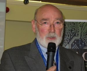
Made welcome by ICT Technical Director Bill Wilkie, delegates were treated to a series of presentations, not only on technology but also on utilisation of social media in business, PCB market analysis, and some of the obstacles to be surmounted in starting a new PCB manufacturing plant in central Europe.
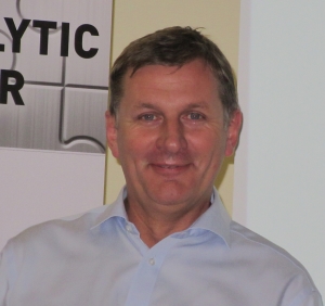
Andrew Barlow from MacDermid Enthone demonstrated how innovations in acid copper electroplating could help overcome some of the challenges of density and thermal management associated with modern HDI designs. Via filling and stacking had become established as a means of increasing interconnection density, but copper-filling of through-holes offered a more reliable process, with improved electrical and thermal conductivity. How could this be achieved by electroplating?
Clearly, substrate thickness and hole diameter were significant considerations, but the two-step process he described had already been shown to be successful for mechanically drilled holes as small as 0.2mm in substrates up to 0.8mm thick, and work was in progress to extend the proven capability to include 0.15mm holes in 0.45mm substrates and 0.1mm holes in 0.35mm substrates. Laser-drilled “X-holes”, popular in mobile phone PCBs, were easier to fill, and nominal 0.15mm holes in 0.2mm thick substrates had been successfully demonstrated.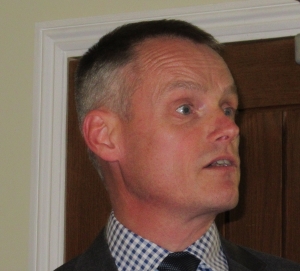
The key first step was to form a copper bridge at the centre of the hole, effectively closing it to create two opposed blind vias, before filling these blind vias with electroplated copper.
A very specialised procedure was required to form the bridges - solution agitation and electrical waveform were critical factors. Banks of eductors gave extremely high solution movement across the surface of the work – a typical working installation had 60 eductors on each side, directly impinging upon the cathode surface with a solution flow of 3 litres per minute per nozzle, and 100 tank turnovers of electrolyte per hour. This solution agitation was combined with knife edge mechanical agitation, with a 10cm stroke at 6-12 cycles per minute
With insoluble anodes and asynchronous PPR rectification specifically tuned to suit the hole sizes being bridged, and anode-cathode spacing of approximately 4cm, best results were obtained if the range of hole diameters was kept to a minimum by the designer. Once the holes were bridged, the via-fill step employed an additive that was preferentially attracted to high-current-density areas so that electrodeposition was favoured at the bottom of the blind vias, so that they became progressively filled with copper without excessive deposition on the surface. Cycle times varied depending on via size, but 75 minutes was typical.
Barlow showed many examples of microsections and x-rays confirming void-free hole-filling, and no cracking or adhesion loss between copper interfaces had been observed after 6 x 10 second solder shocks at 288°C. End markets for the bridge-and-fill technology included IC substrates, LED, military, aerospace and automotive.
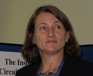
 Dr Despina Moschou, until recently a research fellow at the University of Southampton and currently Prize Fellow in Bioelectronics at the University of Bath gave a fascinating presentation on “Lab-on-PCB” technology for medical diagnostic applications. “In the micro-scale, things change in the fluidics of fluids” she began her introduction to microfluidics: miniaturised systems to bring together microscopic volumes of liquids, transducers and microelectronic components to form biosensors. She went on to describe the characteristics of microfluidic chips, which had micro-channels etched or moulded into a glass, silicon or polymer substrate. The micro-channels forming the microfluidic chip were interconnected to perform functions such as mixing, pumping and sorting, and connected to the outside by inlets and outlets pierced through the chip. The trend towards smarter multi-functional microchips had resulted in the micro total analysis systems known as “Lab-on-a-Chip”: integrated systems of reduced size and weight, performing sample handling steps and analytical measurements faster, at lower cost and with less chance of human error than traditional techniques.
“Lab-on-PCB”, originally suggested in the 1990s as a cost-effective integration platform but side-lined by easier microfluidic fabrication processes, had recently become a main focus of attention because the long-standing industrial infrastructure of PCB technology enabled low-cost upscaling and currently offered adequate microfabrication capabilities: it was not necessary to work at the nanometre scale - 100 micron technology was sufficient.
Dr Moschou illustrated fluidic controls such as microvalves and micro pumps that had been integrated into PCBs, described various biosensor devices and discussed the results of the collaborative ELISA project, which had used exclusively PCB manufacturing techniques to successfully fabricate a 3-layer multilayer Lab-on-PCB measuring 4.6cm x 5.7cm with reference electrodes in layer 1, sensing electrodes in layer 2 and microfluidics in layer 3. There was significant interest both from academia and from industry in further developing the Lab-on-PCB concept.
Ken Ball from techUK, the association representing technical businesses in the UK, took a slot in the seminar programme at short notice with news from the Export Control Reform working group about updates to open general export licences (OGELs) for the export of “low risk” electronics components, which covered PCBs and components for military goods and for PCBs and components for dual-use items. Military OGEL applications covered all countries except Afghanistan, Argentina, Armenia, Azerbaijan, Belarus, Burma, Central African Republic, Democratic Republic of Congo, Eritrea, Iran, Iraq, Ivory Coast, Lebanon, Liberia, Libya, North Korea, Pakistan, People’s Republic of China, Russian Federation, Somalia, South Sudan, Sudan, Syria, Yemen and Zimbabwe. He also commented on business issues regarding digital licencing and apprenticeship levies, and that techUK was seeking opinion from British industry on the possible consequences of “Brexit”, in order to feed concerns back to government.
The seminar took on a different dimension when Daniel Knowlton literally leapt into action with an energetic and animated promotion of socia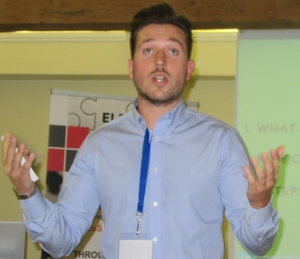 l media as tools for growing businesses. “Get to grips with digital marketing, it’s hugely, hugely, hugely powerful! After today you will all be inspired to use social media!” he confidently predicted. “Marketing is all about attention. It used to be print and billboards – if you’re not changing with the times, you’re going to get eaten up. Become part of an on-line community – it’s a great way to develop presence and brand awareness, build relationships and generate sales! Become a key centre of influence! The average user spends 2.3 hours a day on social media – people are forever checking their phones to be up to speed with what’s happening and to make sure they’re not missing out!”
“Who is this bloke, and why should I listen to him?” was the rhetorical question he asked the audience, before cataloguing his credentials, which included being one of the world’s top 100 influential people in digital marketing and having won an award as social media business of the year.
While moving around a lot, talking very fast and referring to strange-sounding websites, he commanded the attention of the audience as he listed five steps to social media success: Step 1, find out who are the highly influential people in your industry, using sites like Followerwonk, and what information they are sharing, using sites like Buzzsumo, Socialmediaexaminer, Bufferblog and Blog.Bufferap. Step 2: Use free resources to learn. Step 3: Follow the influencers. Step 4: Create an action plan. Step 5: Measure success using social media analytics like KLOUT.
Son of business improvement specialist Mark Knowlton, a popular contributor to ICT events on the subject of Lean Manufacturing, Daniel Knowlton certainly left an impression on his audience. How applicable his techniques would be in the high-end electronics business, how inspired the specialist PCB manufacturer would be to use social media to supplement his direct technical sales effort will remain to be seen. The community printed circuit board platform Ragworm has already demonstrated the effectiveness of social media in driving its basic PCB prototyping service. Maybe the industry establishment should open its eyes, take notice of the ideas of an eager up-coming generation and recognise the influence they will have on the industry’s future….
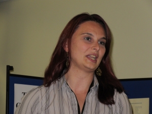
 Back to normality: market analyst and ICT council member Francesca Stern gave her latest outlook on the PCB and electronics industries, based on UK and global trends in electronics production and the PCB production supporting it. Excluding components, global electronics production in 2015 was £980 billion, of which Europe’s share was about £150 billion with the UK contributing about £12.5 billion. UK PCB production in 2015 had been estimated at £125 million, against a market demand in excess of £168 million.
Electronics equipment production in Europe and North America remained relatively strong in industrial, instrumentation and automation in 2015, whereas military expenditure had been low to flat but was forecast to creep up in 2016. UK electronics production had declined slightly in 2015 and continued to decline in the first half of 2016, more in the export market than the home market. PCB production had declined in Europe in 2015 and there had been some recovery in 2016 but no growth yet, although it was forecast to go positive in late 2016 or early 2017. PCB production in the UK was following a similar trend. There was low growth in North America and further decline in Japan. Measured in domestic currencies, there had been some growth in Asia but exchange rate changes meant that this was negative if converted to US dollars.
 Exchange rates were a sensitive topic as the seminar programme concluded with the last-minute arrival of dare-to-be-different SCL PCB Solutions Group CEO Steve Driver, just back from Romania with an update on his PCB factory start-up there and comments on the repercussions of the “Brexit” referendum. In his opinion, the decision to leave the European Union was horrible news, and a lot of damage had already been done to the UK and to the PCB industry. For a company like Spirit Circuits, a significant proportion of whose business involved imported PCBs paid for in US dollars, the plunge in the value of the pound had major financial consequences. And imported materials and equipment would inevitably cost more - all hurting cash flow and profitability. “We’re all in the same boat – we just have to keep calm, hunker down and take actions!”
What was the latest on the Romanian enterprise? “I’ve never worked so hard!” Romanian bureaucracy continued to frustrate his efforts to get the operation into production. He had only gained access to the industrial unit three weeks before, and his advance team of 16 people was working round the clock to get the basic factory infrastructure into place – cleaning, digging holes, laying concrete. And Driver was still awaiting formal authorisation to use the building for PCB manufacture. “The principle of it being better to seek forgiveness than to ask permission doesn’t work in Romania!” he commented, taking as an example a document 142 pages long with stamps – “they’re obsessed with them!” – on every page. The bureaucracy was also causing delays in obtaining waste water permissions and establishing electricity supplies.
But Driver was determined to see the project through. The advance team had undergone 6 months training in the UK, the plan was to extend the workforce to 41 by January 2017 and to 100 later in the year. Three trucks-full of equipment were already in Romania, another five were loaded and ready to go, and pilot production was scheduled to start in December. Steve Driver thrives on challenges, and no-one in the room was in any doubt that the obstacles would be overcome one way or another.
Hayling Island lived up to expectations - once again an excellent technical seminar and learning opportunity, a tribute to Bill Wilkie’s organisational skills and the generous support of Macdermid-Enthone and Spirit Circuits, and a premier be-there-or-miss-out networking event for the UK PCB industry.
Pete Starkey
I-Connect007
September 2016