A return to the historic spa town of Harrogate in Yorkshire, England for the Institute of Circuit Technology Northern Seminar, to enjoy a diverse programme of presentations on safety standards, research in selective metal deposition, and developments in imaging and inspection techniques.
 After extending a warm welcome to delegates and acknowledging the support of sponsors Fineline VAR, ICT technical director Bill Wilkie began by reminding members of the value of the Institute website as a source of essential information. He made particular reference to the BSI page and recent controversy about proposals by IEC TC111, where as a result of the Institute’s representation on BSI standards committees, members had early warning of a potential ban on PTFE laminates, which put them in a strong position to lobby against it.
View Emma Hudson's Presentation
He introduced as first speaker the ever-popular Emma Hudson, Lead PCB Engineer for Europe and Latin America with UL,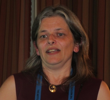 who has made it her vocation to help the PCB industry through the safety certification process. Her topic was Solder Limits, and bringing them up-to-date in respect of surface-mount assembly processes. The thermal stresses experienced in surface mount assembly could be considerably more severe than those typically represented by a traditional solder-float test. Therefore for an accurate safety assessment of the PCB, it was essential that Solder Limits meaningfully represented the actual soldering processes the PCB would be exposed to during assembly operations. If the Recognized Solder Limits were exceeded in production then the Recognition, in effect the safety assessment, would be invalidated, because the more severe the soldering operation, the greater the degradation in the properties of the PCB evaluated for safety.
Hudson made it clear that UL acknowledged the existence of many different product-specific soldering profiles, and the difficulties faced by PCB manufacturers in choosing which profiles to use for Recognition to meet all their customers’ needs. In an effort to help the industry, UL would be offering standardised soldering profiles for Solder Limits to make their implementation easier. These were based on IPC-TM-650 2.6.27 T230 and T260 reflow profiles as a default option to represent tin-lead and lead-free SMT soldering, although bespoke profiles and additional wave-solder-type soldering limits could be requested. And UL were also attempting to add a reference to these profiles into UL 796 for guidance.
She described the procedures for updating Solder Limits for different base materials and multilayer constructions, explaining where the CCIL Program could and could not be used, and went on to discuss procedures for solder resist, with examples of when the Permanent Coating Program could and could not be used. And she urged PCB manufacturers to push their suppliers to Recognize their materials with suitable Solder Limits. Furthermore, she strongly recommended Recognizing any new PCB with the new solder limits, whether materials were Recognized with these requirements or not, and to contact UL for assistance sooner rather than later. “Do it before your customer contacts you!”
UL aimed to actively inform all relevant parties: PCB manufacturers, material manufacturers, Recognized PCB assemblers and OEMs with UL Listed products. UL follow-up services would commence in 2018, and UL would require to see evidence of the actual soldering profiles used for the PCB assembly, to confirm that the soldering processes to which the PCB had been exposed did not exceed the Recognized solder limits and so invalidate the Recognition.
View Andy Cobley's Presentation
The second presentation came from ICT Chairman Andy Cobley, recently appointed Professor of Electrochemical Deposition at Coventry University, who gave an insight into current research on magnetic-field-enabled selective metallisation of dielectric substrates.
Previous research on the effects of a magnetic field on electrochemical deposition had demonstrated that placing a magnetised iron template behind a conductive substrate induced a magnetohydrodynamic effect which caused changes in the distribution, morphology and crystal structure of electroplated metals, and offered scope for selective deposition. The current work studied magnetic and magnetohydrodynamic effects in the electroless deposition of metals on non-conductive substrates as a potential means of creating conductive patterns. Cross-sections of electroless nickel-boron deposited with and without an applied magnetic field showed significant differences in grain structure, and the magnetic field gave an increase in deposition rate.
Classical electroless deposition on a non-conductive surface required a catalyst such as colloidal palladium to initiate the reaction, but this had no magnetic properties. Therefore a material was sought which had both catalytic and magnetic properties, and it was attempted to design and synthesise magnetic/catalytic nanoparticles that could be selectively deposited on a non-conductive substrate using a magnetic field, and to demonstrate that these would initiate electroless copper deposition. The concept was to produce particles with a magnetic core and a catalytic shell, based on Fe3O4 iron oxide and silver, by a two-stage process starting with ferrous sulphate and silver nitrate and using arginine as reducing agent. In the event, the resulting nanoparticles were shown to be a composite, with the silver predominantly in the core. However, they proved to have catalytic properties, and to successfully initiate electroless copper deposition. Their efficiency varied depending on concentration, dispersing agent and pH.
Initial trials had shown that the particles could be selectively deposited on a thin FR4 substrate by placing a magnetic template behind it, and electroless copper could subsequently be deposited on the catalysed area. Proposed future work included further study of the magnetic properties of silver-iron oxide nanoparticles, the synthesis of copper-iron oxide nanoparticles as an alternative to silver, and the removal of iron by dissolution after selective catalysation and before electroless deposition, as well as a comprehensive investigation of the effects of process parameters. Coventry University’s IP had been secured by patent, and the team was keen to find commercial partners and to identify possible applications of the technology.
In the third presentation, Jean-Paul Birraux, sales and marketing manager with First EIE in Switzerland, discussed developments in photo-plotters, UV direct  imaging and automatic visual inspection systems.
He commented that when he first joined the company in 1999, its former president had predicted that the market for photoplotters would continue only for five years before direct imaging technology would make silver halide films obsolete. In fact the present-day photoplotter market remained strong and there was a demand for higher resolution, higher speed and larger format machines, driven by the manufactures of shadow masks and OLED screens, for example 2.4m x 1.6m with +/- 10 micron accuracy. There was increasing use of long flexible circuits as replacements for wiring harnesses in automotive and avionics applications, and in development was a plotter with unlimited length capability for applications in this sector.
Meanwhile there had been ongoing development in direct imaging technology, and again the trend was to larger-format machines for panel sizes up to 6m x 1m. Light sources with a continuous spectrum from 360nm to 450nm gave a good combination of surface cure and through cure on solder masks. Advances in digital-micro-mirror-device (DMD) technology, using a collimated UV arc-lamp source and a single DMD head, offered a cost-effective and low-maintenance option, enabling very high exposure energy, up to 1000 mJ/cm2 with 20 micron line and space capability.
And in the field of machine vision systems, a new generation of automatic visual inspection equipment had been developed, with the capability to create a master reference image from a single sample, and to inspect both sides of a 240mm x 240mm circuit in a third of the time taken by a human inspector, capturing defects to the 20 micron level. There was also an increasing demand for continuous roll-to-roll inspection.
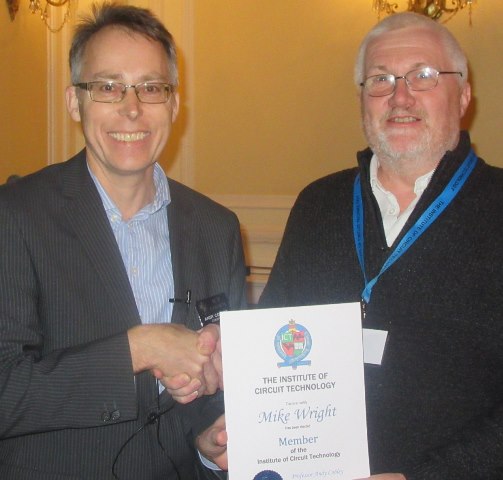
Andy Cobley brought proceedings to a close and presented Mike Wright, Global Quality Representative for DK Thermal, with his Membership certificate.
As ever, the ICT Northern Seminar provided a platform for the dissemination of knowledge, the sharing of experience and the broadening of a network of PCB professionals. And thanks again to Bill Wilkie for his hard work in organising and coordinating an excellent event.
Pete Starkey
I-Connect007
December 2017

