ICT Winter Seminar ReviewDecember 7, 2021 - Pete Starkey, I-Connect007 |
|
 |
Faced with the choice between a real or virtual event, Bill Wilkie took a calculated risk. It has been many long months since members of the Institute of Circuit Technology had gathered together under one roof, but a fair-sized bunch of industry stalwarts braved the weather and the threat of COVID, descended on the Manor Hotel in Meriden, UK, on November 30, and applauded Bill’s decision to go live. They were not disappointed; the program was superb, the atmosphere upbeat, and the networking opportunity priceless. |
|
|
1. Advances in X-ray Metrology
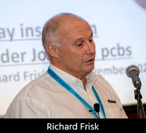
Frisk briefly introduced the company, which had three other specialist divisions: imaging products, semiconductor lithography systems, and healthcare, in addition to their interests in industrial metrology. He commented that the Nikon name derived from “Optics from Japan.” Although X-ray imaging systems had been used for many years as an aid to PCB manufacturing, their main historic application had been for checking registration in multilayer boards. There had been many advances in capability over the last 20 years and Frisk described three types of X-ray image that had particular uses in solder joint inspection: radiography, computed tomography and laminography. He emphasised that, for metrology, good image quality was the basis for accurate measurements. Using radiographs of a soldered BGA device, he demonstrated how radiography was used to detect and measure voids in the solder joints, explaining that it had become normal practice to invert the image so that the denser the material the darker it would appear and voids would show as light within a dark background. A view with the X-ray source and detector normal to the PCB showed clearly defined solder balls and bond wires. Some solder balls showed evidence of voids and it was possible to calculate the percentage of solder ball area to void area and apply accept-reject criteria to the images. An oblique view gave the effect of seeing the image in perspective and enabled voids to be further classified as “near to the PCB-solder interface,” “near to the IC-solder interface” or “mid-ball,” and features like poorly formed solder joints and head-in-pillow type defects could be identified. Resolution was high enough to enable wire-bond and die attach inspection, and the examination of individual balls. Typical X-ray settings were 110 kilovolts and 130 microamps. He showed several analysis examples and inspection algorithms for BGA devices, although he commented that radiographs could get very “busy” and needed a skilled operator to make judgements. Computed tomography was a scanning process whereby the sample was continuously rotated whilst thousands of X-ray images were taken and then reconstructed by a powerful computer into a three-dimensional volume from which two-dimensional slices could be sectioned in any direction and a three-dimensional model generated, enabling in-depth automated defect analysis and measurement at high resolution. Individual materials could be colour-coded and Frisk’s examples of the structure of QFP and BGA components were spectacular in their detail. With flat samples such as PCB assemblies, a limitation of computed tomography was the distance that could be fully penetrated as the sample was rotated parallel to the X-ray beam. In comparison, laminography was a non-destructive inspection technique for samples of any size that enabled the virtual micro-sectioning and analysis of large boards with typical scan times of less than five minutes. Laminography could be used to view defects in multi-layer PCB assemblies and devices and for early identification of latent defects. Frisk held the audience spellbound with some video examples of fault-finding and forensic applications which demonstrated the capability and versatility of currently available X-ray equipment. |
|
|
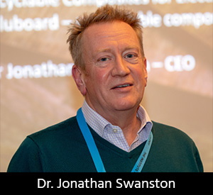
2. A Solution for E-Waste?“The world’s first recyclable PCBs” were features of the presentation by Dr. Jonathan Swanston, CEO of Jiva Materials, originators of the Soluboard recyclable PCB substrate. Swanston began with the frightening statistic that 54 million tons of waste electronics and electrical equipment are produced world-wide annually, and the quantity continues to grow. His figures indicated the UK alone to be responsible for generating the equivalent of 23.9 kilograms per person, a total of 727,000 tons, and that 32% of all e-waste consisted of small domestic equipment. Against that background, he described the characteristics of Soluboard, a composite laminate based on natural materials bound by a non-toxic and biodegradable resin soluble in hot water, with physical properties comparable to those of market leaders. The carbon footprint of one square metre of Soluboard was equivalent to 7.1 kg of carbon dioxide, compared with 17.7 kg for one square metre of standard FR-4, indicating a 60% reduction in carbon footprint and a saving equivalent to 620g of plastic per square metre compared with FR-4. Swanston described two versions of his material, a copper-clad laminate for subtractive processing, with woven fibre reinforcement based on jute, and a bare laminate for printed electronics with woven fibre reinforcement based on flax. The manufacturing sequence for the unclad version followed similar impregnation, drying, layup and press lamination stages to those used in conventional laminate production. Copper foil could be subsequently press-bonded to unclad material using an adhesive. The process stages for producing PCBs were basically similar to standard practice. Conductive silver ink was used for assembly of printed electronics substrates and low-temperature solder for etched circuits. He showed an example of a fully assembled prototype single-sided Arduino board produced by Jiva Materials. It was believed that the mechanical and electrical properties of Soluboard would meet the requirements of most sectors within the electronics industry. Testing to IPC standards was in progress and expected to be completed shortly, with UL recognition to follow during 2022. Jiva’s initial target market was a share of the 2.8 billion square metres of FR-4 currently used in single and double-sided boards for domestic appliances. |
|
|
3. Electronics Research ProjectsAlthough gaining access to the third presentation may have tested Bill Wilkie’s IT skills, his efforts were rewarded when the connection was successfully made and a virtual presentation was received online from Martin Wickham, senior research scientist at the National Physical Laboratory. It was clear that there was a lot going on at NPL. Wickham gave an update on a busy program of new electronics research projects meeting current challenges in electronics reliability. Smaller, lighter, faster, cleaner, smarter, hotter—these were the inevitable buzzwords, reducing CO2 emissions toward “net zero” was a major driver and there was general push toward higher voltages. One of the main projects in the 2021-2022 program was the continuing study of high voltage “partial discharge” effects, which could occur as a “spark” in the insulation between two conductors at a point where the electric field exceeded the local dielectric breakdown strength and was often associated with minor defects in the dielectric. Partial discharge could occur multiple times at lower voltages and progressively reduce the breakdown strength of the insulation. A multi-channel test system had been developed and used for an initial evaluation of partial discharge and insulation resistance at high voltage. The system could operate at voltages up to 10,000V. Work to date had concentrated on twisted pairs representing motor insulation but would shortly be extended to include PCBs. The second phase of the ongoing study of conductive anodic filament (CAF) effects at high voltages had recently been completed. Test boards with different design details for CAF and surface insulation resistance (SIR) monitoring had been aged at 1000V DC, with hole-to-hole distances in the range 550 to 2100 microns for CAF and pad-to-pad distances of 440 to 1950 microns for SIR. All the CAF patterns had failed within 2,000 hours but there had been no SIR failures for the three no-clean solder pastes tested. The time to failure for CAF was inversely related to DC voltage. NPL had proposed a multi-partner project for investigating CAF failure, and IPC had organised a round robin on the prevention of SIR failures in CAF testing. Electrochemical impedance spectroscopy had been utilised for rapid materials evaluation. This used AC impedance to determine the impact of flux residues, as an alternative to traditional DC SIR measurement. It was expected that its predictive capability could be developed into a non-destructive test method. Wickham also briefly discussed developments in fast turnaround insulation resistance testing in damp environments, platen condensation testing, immersion testing and rapid in-process conformal coating evaluation, as well as a new measurement facility and test vehicles for the quick assessment of reliability of coatings under harsh conditions. Industry collaborators were invited to join a multi-partner project to evaluate electronic materials for harsh environments. |
|
|
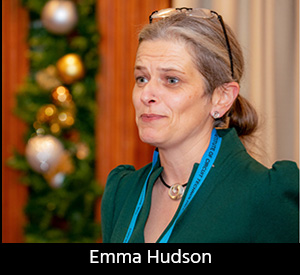
4. Solder LimitsThe final presentation, forewarning the industry of imminent changes in UL solder limits, came from ICT Chair Emma Hudson. Urging material suppliers and PCB fabricators to get prepared without delay, she explained that solder limits were key parameters for UL Recognized PCBs, representing the soldering processes to which the PCB would be exposed during assembly operations and capturing all time spent over the maximum operating temperature and the maximum temperature reached. They were employed in many of the test procedures used to characterise a PCB as part of the recognition process. Hudson stressed that if solder limits were exceeded during PCB assembly, the safety evaluation conducted on that PCB was invalidated. Reviewing current status, she explained that the new editions of standards UL 796 for printed wiring boards, UL 796F for flexible circuits, UL 746E for laminates and coatings, and UL 746F for flexible materials, recently published, had all included standardised solder limits and assembly solder process requirements. These defined all the time spent over the maximum operating temperature, or 100°C whichever was greater, and the maximum temperature reached as measured on the surface of the PCB. The standards now included a new default solder process condition: six cycles of the IPC T260 profile. UL had issued a bulletin to all manufacturers with PCBs Recognized under UL 796 and UL 796F explaining the concept of standardised reflow profiles, the updates to the standards and how they would be implemented. UL Follow-Up Services would verify at the assembly company that any board certified from January 1, 2022 had suitable solder limits and assembly solder process parameters for the actual process, and if any PCB was not Recognized with the appropriate parameter it would be deemed a non-conformance. Any changes or modifications to existing PCB types, including the addition of new materials, conductor parameters, solder limits, maximum operating temperatures and flammability rating made from January 1, 2022 would also be subject to the new inspection criteria. Existing board types that remained unchanged could be left as they were. Hudson highlighted the need for laminate and solder resist manufactures to update their materials to the new solder limits and assembly solder process parameters, preferably to the default of six cycles of the T260 profile, otherwise the PCB manufacturers would face much more testing. She advised PCB manufacturers to talk to their laminate suppliers without delay about their plans to upgrade their material Recognition. Some testing would still be needed to upgrade PCBs to the new assembly solder process solder limits but if materials had the new values the amount of testing could be reduced. Similarly, solder resist suppliers could adopt the default assembly solder process parameters and their associated flammability testing requirements. She suggested that PCB manufacturers who had impending changes to existing PCB types should consider the creation of duplicate types in their UL files, making copies that could then be updated as and when necessary, depending on the ease of maintaining the PCB type designation with their customer. Her closing words were: “Be prepared as a PCB manufacturer. This is happening. Ask your material suppliers what they are doing to help you.” The Institute of Circuit Technology Autumn Seminar 2021 was a great success. It provided an excellent technical programme and much more. It was a gathering of real people and a long-awaited networking opportunity. |

