ICT/IeMRC Plating Technology Seminar. Loughborough University 6 August 2008
(Visit the Download Presentations Page to view the 6 presentations).
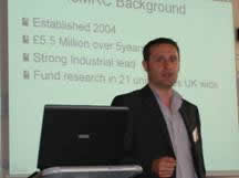 Classic English summer - grey skies and rain! But the crowd of eager delegates who gathered at the Wolfson School of Mechanical and Manufacturing Engineering in Loughborough University were there to learn about state of the art metal finishing processes for PCB manufacture, not to escape the weather. The Institute of Circuit Technology joined forces with the Innovative Electronics Manufacturing Research Centre for a Summer Seminar on Plating Technology, introduced by IEMRC Co-ordinator Dr Darren Cadman and ICT Technical Director Bill Wilkie
 Dave Wayness from Rohm and Haas explained in detail how cost and performance of copper electroplating processes could be optimised for different applications, with a sage reminder that technologies could be easily over-sold and that it was important in choosing the right process to understand not only what it did well but also what it did not do well! The days of one-process-fits-all were long past and even different geographical regions now required significantly different functionality to support the design characteristics and end-user requirements of their particular market sectors. He reviewed many permutations: vertical or horizontal processing; DC or pulse rectification; panel, semi-panel or pattern plating; conformal plating or microvia filling; soluble or insoluble anodes, and described how Rohm and Haas had developed a series of copper plating chemistries to achieve specific objectives in high aspect ratio through-plating and via filling, defining “difficulty factors” and “stability indices” to gauge their effectiveness, and using a mathematical model to calculate the cost savings which could be achieved using the appropriate process variant for the job.
 Jean Rasmussen from Cookson described the technical and environmental benefits of direct metallisation using intrinsically conductive polymers to selectively activate resin and glass without contamination of copper surfaces. Cookson’s process worked by first depositing an initiator layer of manganese dioxide, which then acted as an oxidative initiator for the in-situ polymerisation of ethylene-dioxy-thiophene in the presence of an organic sulphonic acid. The conductive polymer was mechanically and thermally stable, and in high-aspect-ratio through-holes, coverage with acid copper was complete and void-free within 60-90 seconds. The process had significant environmental advantages when compared with electroless copper. It contained no formaldehyde or chelating agents, waste treatment was simple and large savings could be made in water consumption, making it particularly attractive to Asian fabricators for whom water was generally a very expensive commodity.
 Andy Cobley, sonochemistry specialist from Coventry University, reviewed studies of the physical and chemical effects of ultrasound in liquid media, and their potential applications in metal finishing, where traditionally ultrasonics had been used only for cleaning purposes. Explaining the principles of acoustic cavitation, theoretically capable of generating enormously high pressures and temperatures at the point of collapse of microscopic bubbles, and the phenomenon of microjetting, when bubbles collapse asymmetrically at a surface, he demonstrated how increases in limiting current density and current efficiency could be achieved in electroplating as a consequence of disruption of the diffusion layer. In electroless copper plating, the use of ultrasonics simply at the catalyst stage gave a significant increase in the deposition rate of copper, and this increased further if ultrasonic agitation was applied in the copper bath as well. This effect could possibly be exploited in the development of formaldehyde-free electroless copper chemistry.
Martin Bunce from MacDermid described recent advances in electroless copper process technology. MacDermid’s whole sequence had been designed specifically to maximise the reliability of inner-layer connections, and began with an organo-silane conditioner, which was adsorbed only on to non-conductive surfaces. A tin-palladium catalyst reacted with the conditioned surfaces, whilst depositing very little on copper. The accelerator was unusual in that, instead of dissolving-away the stannous tin, it oxidised stannous to stannic and left it in place as a shield to the palladium nuclei, resulting in slow, controlled initiation of electroless copper. The copper chemistry gave a low-stress deposit with fine grain structure and minimal co-deposition of contaminants. Solder shock and interconnection stress testing demonstrated that, even after the most severe thermal abuse of high layer-count test boards, the interconnections between plated-through-hole and inner layers maintained their integrity.
 Brian Reid from Schloetter gave a practical account of the development of an acid copper electroplating process to satisfy the demands of smaller UK PCB fabricators who wanted a via-fill process that could be used simultaneously for pattern plating, on standard equipment, with soluble anodes. The result was a high-copper, low-acid formulation with three liquid additives, which combined excellent levelling with good ductility and low internal stress. Typical cycle time was two hours at 1 amp per square decimetre for via filling in pattern plating mode. Although insoluble anodes gave the most consistent results, they were comparatively expensive and soluble copper anodes could be successfully used provided they were removed from the electrolyte during idle periods.
Pete Starkey,
ICT Council.
