New Developments in PCB and Interconnect Manufacturing
Rotherham, UK, 4th August 2009
Over forty leading representatives of industry and academia gathered at the National Metals Technology Centre, in Rotherham, South Yorkshire, England, to attend a seminar entitled New Developments in PCB and Interconnect Manufacturing. The event was hosted by EY, and supported by IeMRC and the ICT.
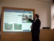 After welcomes and introductions from Dave Williams, Business Development Manager of EY, Dr Darren Cadman, Research co-ordinator of IeMRC, and Steve Payne, Chairman of ICT, Professor Martin Goosey introduced the keynote speaker, Professor David Selviah of the Department of Electronic and Electrical Engineering at University College London., who explained the objectives of the IeMRC Opto-PCB Manufacturing Project and gave an overview and update of the results and achievements of the project partners: three universities and eight industrial collaborators.
Driven by the need to reduce loss and eliminate crosstalk between copper conductors on high-data-rate backplanes by the use of optical waveguides, but accepting the reality that optics cannot transmit electrical power, the project sought to develop techniques of integrating optical and electronic interconnect into functional structures using processes compatible with those established in printed circuit fabrication. The focus of the OPCB project was to produce a 19 inch PCB with multimode waveguides working at up to 10 Gb/s with in-plane butt-connections to VCSEL transmitters and detectors. A variety of techniques and materials had been used in fabricating optical waveguides, including direct laser-writing with a 325nm Helium-Cadmium laser on photo-polymerisable acrylic resin, laser ablation using Excimer, Nd-YAG and CO2 lasers on acrylic or polysiloxane resins, inkjetting with UV-curable polymer, and photolithography. In addition to the work on fabrication techniques, methods had been developed for characterisation of waveguide performance, by modelling and by measurement, to enable design rules to be formulated for incorporation into PCB CAD systems. Professor Selviah showed several examples of demonstrator assemblies together with their performance data: crosstalk, optical loss and misalignment tolerance.
Pete Starkey, on behalf of EIPC, gave an introduction to the EU-funded SurfEnergy, IONMET and ProSurf projects. Against a background of the European PCB industry having contracted over the last decade to leave around 400 manufacturers producing about 7% of world output, and most of these manufacturers being small-to-medium enterprises, the future of the industry lay in innovation, cost reduction and environmental safety. The European Commission had made funding available through FP6 and FP7 Framework Programmes to promote scientific excellence, improved competitiveness and innovation in the field of research and technological development. EIPC were involved in three Framework projects: SurfEnergy, a new project to provide advanced tools for surface finishing processes to optimise energy efficiency, IONMET, a project nearing completion focused on radical new developments in metal finishing using ionic liquid solvent technology, and ProSurf, a recently completed project promoting and supporting SME research and innovation in the surface finishing and printed circuit manufacturing sectors. One outcome of the ProSurf and IONMET projects was the PCB Technology Roadmap report, which was available from EIPC.
 Dr Andy Cobley of the Sonochemistry Centre at Coventry University gave a presentation entitled Sonochemical Surface Modification of Electronic Materials.
Taking as his point of reference the traditional chemical process sequence for de-smearing and texturising epoxy-glass surfaces, with associated concerns of hazardous chemistry, VOCs, carcinogens, corrosives, rinse water consumption and waste treatment costs, he demonstrated what could be achieved using only water in conjunction with ultrasound. Explaining the phenomena of ultrasonic cavitation and micro-jetting, and demonstrating that ultrasound in water could cause aluminium foil to disintegrate, he described how significant sonochemical surface modification could be achieved on a variety of materials used in electronics manufacture: FR4, polyphenylene oxide/polystyrene, ABS and ceramic. The project had identified a number of influencing factors, including frequency, ultrasonic intensity, probe-to-sample spacing, liquid temperature and the effect of adding surfactant. Optimistaion of conditions had reduced process times and increased weight loss by factors of 4, and the technique presented a technology platform from which potential commercial applications were emerging.
 Chris Rogalski from Coretest Technologies described a novel anisotropic conductive fabric consisting of minute silver-plated nickel spheres embedded in a silicone rubber.
With a video, he illustrated how, under a magnetic field, the spheres were aligned into discrete “ball-wires” in the z-axis during the manufacture of the material, to give a membrane with 30 to 50 contacts per 1mm square at 0.38mm thickness, scalable down to 30 to 50 contacts per 0.1mm square at 0.06mm thickness for wafer-scale applications. The material was characterised by very low contact resistance and high bandwidth, with fast rise-time and low inductance and capacitance, and less than 0.3dB loss at 40GHz. Proven interconnection applications included test and burn-in, flip-chip packaging, sockets, flex circuit connectors, battery contacts and snap-together housing connectors. New applications continued to emerge. The material could be cut to any shape, and could be used as an RF gasket or for optical devices where a viewing window was required.
 Dr David Hutt of Loughborough University had been investigating the practicability of using glass as an alternative to organic substrates in the fabrication of multilayer interconnects for high-density devices. A space-grade glass, designated CMZ and available in thicknesses of 50 – 150 microns, with expansion coefficient close to that of silicon, had been chosen as the base material. This had been machined with a pulsed 248nm Krypton Fluoride excimer laser, using mask projection to produce fine grooves for conductors and waveguides, and microvia holes. Challenges included re-melt, debris, hole taper and microcracking, and these had been minimised by careful process optimisation and the use of a protective film. Electroless copper and electroless nickel had both been successfully deposited onto smooth glass surfaces, and further work was in hand to improve adhesion, using self-assembled APTS monolayers as adhesion promoters. Metallisation of laser-machined areas gave comparatively good adhesion, and if a photoresist was used during laser machining of the conductor pattern, this could act as a mask to define the initial APTS image so that catalyst was attracted selectively to enable full-additive circuit formation. Glass layers had been successfully laminated together without the use of adhesive, by pressure-assisted low temperature bonding, and multilayer interconnects were in prospect.
 Nigel White, European Product Marketing Manager with Atotech, explained the benefits of electroless nickel/electroless palladium/immersion gold as a selective finish for soldering and wire bonding, and how four different process variants had been engineered to suit specific applications: the IC substrate industry; PCB customers who wished to supplement their existing ENIG lines with a palladium-phosphorus stage; medical, military and aerospace requirements for pure palladium, and low-temperature co-fired ceramic manufacturers needing to plate on ceramic/silver paste materials. Nickel/palladium/gold had been demonstrated to give improved solder joint integrity when compared with ENIG, and significant cost savings over electroplated nickel/gold as a wire-bonding finish. White gave a detailed description of the process chemistry and deposition characteristics, and illustrated the fundamental differences between immersion and electroless palladium: electroless giving a more uniform deposit with no corrosive attack at the grain boundaries of the nickel-phosphorus layer. The nickel/palladium/gold finish was gaining wide acceptance with PCB, semiconductor and co-fired ceramic producers.
 Russ Crockett from DuPont began his review of the latest developments in dry film photoresists for laser direct imaging by posing the question: “Is LDI an enabling technology to improve production capability, or a route to cost reduction through yield improvement?” The answer was Yes in both cases, depending whether the user was in small batch quick-turn or in volume production of HDI on large panels. He stressed that LDI was not the only factor in producing a perfect photoresist image – it was one of five process steps, each of which needed to be properly engineered and controlled if a satisfactory result was to be achieved. Discussing the different LDI systems available, principally those based on polygon mirrors working at a wavelength of 355nm and those based on digital micro-mirror devices working at 405nm, he explained the difficulties in producing a dry film photoresist which would suit both applications whilst maintaining acceptable photospeed, adhesion, resolution and processability, and why DuPont had chosen to formulate specialist products to suit specific applications. He illustrated the performance of state-of-the-art dry films with a series of photographs of cross-sections and sidewalls, together with a statistical analysis of the yield improvements in image defects and registration achieved by LDI.
 Final presentation was a detailed overview of solder mask processes and properties from Chris Wall of Electra Polymers. Starting from first principles he explained how to choose appropriate materials, application and imaging systems to suit particular PCB design technologies and performance requirements. He described how rheological characteristics needed to be optimised to match each of the three principal application methods for liquid photoimageable solder mask: flood-screen printing, curtain coating and high-pressure low-volume air spraying, which he compared in terms of coverage profiles, via plugging, hole cleaning and environmental considerations. He discussed the practical aspects of resolution and registration, and presented the results of comparative tests to demonstrate the ability of a processed solder mask to maintain 10µm on track edges, wash clean 0.2mm via-holes and maintain 50µm solder dams. Solder masks were required to conform with specifications such as IPC-SM840, MIL-P55110 and Bellcore, to withstand the process chemistries associated with ENIG finishing, and the temperatures involved in lead-free soldering, as well as being compatible with fluxes, cleaners, underfills and adhesives.
The town of Rotherham has historically been associated with coal and steel, but time moves on and these industries have largely faded away. This seminar exemplified how non-profit organisations like EY (formerly Electronics Yorkshire) are supporting and promoting the growth of the region’s electronics industry with IPC-authorised skills training in electronics assembly and an active participation in the Electronics Knowledge Transfer Network. Certainly a great deal of knowledge was exchanged and the industry/academia contact network was extended by this joint EY/IeMRC/ICT event.
Pete Starkey
