
Institute of Circuit Technology Seminar, Sandbach 3rd March 2015
 Sandbach, in Cheshire, UK, was the venue for the well-attended Annual General Meeting of the Institute of Circuit Technology, followed by an informative and enlightening seminar programme introduced by Technical Director, Bill Wilkie.
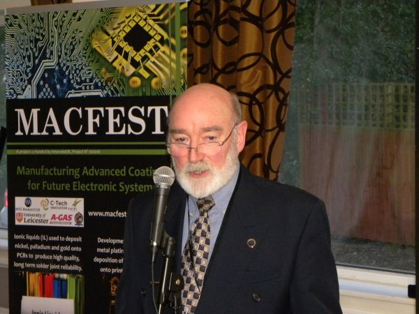
Retiring ICT Chairman, Professor Martin Goosey reviewed the ICT's two current multi-partner R&D projects, STOWURC and MacFest, which addressed key issues of interest to the UK PCB industry and were both part-funded by Innovate UK (formerly the Technology Strategy Board). He commented that the bizarre acronyms were a consequence of the supervising authority's requirement for short names that reflected the theme of the project. So STOWURC stood for Sustainable Treatment of Waste Using Recycled Chitosans, 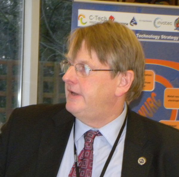 and MacFest for Manufacturing Advanced Coatings for Future Electronic Systems.
The principle of the STOWURC project was to use waste from one industry sector to treat waste from another industry, specifically to use materials derived from crab shells to treat metal-bearing effluent from the PCB and metal finishing industries. The two-year project was currently past its half-way stage, and due to finish at the end of November 2015. The project consortium covered the whole supply chain, from raw material to dissemination, and included a crab-fishing and dressing company as raw material supplier, a chemical process supplier, a printed circuit board fabricator, a research and technology exploiter and a process equipment fabricator. The Surface Engineering Association and the Institute of Circuit Technology were responsible for disseminating the results and conclusions.
Professor Goosey explained that the requirement to remove low levels of metals from PCB manufacturing effluent could be achieved by using ion exchange resins but that certain natural products could also absorb these metals. The STOWURC project was investigating the use of a natural waste product to both capture and recover metals from effluent. Chitin, a long-chain polymer of a N-acetylglucosamine, was a constituent of crab-shells which had the ability to adsorb metals such as copper from dilute solution. Chitosan, a derivative of chitin produced by a deacetylation treatment, was a more effective adsorbant. And once adsorbed, it was possible to elute the metal and recover it by electroplating. He showed how the rates of copper absorption compared for crab-shell, chitin, and chitosan, and how they varied depending on solution parameters such as temperature, pH, initial concentration, rate of mixing and metal speciation, and chitosan parameters such as amount of adsorbent, degree of deacetylation and particle size. Copper had been desorbed and recovered by conventional electroplating techniques and the materials had been evaluated through multiple cycles. The project was currently focused on optimising materials and processes for specific applications.
The two-year MacFest project had begun in January 2015 with the objectives of developing solderable finishes with improved solder joint reliability in harsh environments, whilst reducing the toxicity of chemicals used in PCB manufacturing processes and reducing energy input, and was based on deposition of metals from ionic liquids. The initial objective was the development and evaluation of new nickel-palladium-gold solderable coatings. Full literature and IP searches were currently being undertaken, together with an assessment of actual end user requirements, and trial formulation and deposition studies were under way at the University of Leicester.
 Next presentation, entitled "Thermal management: the role of substrate", came from Geoff Layhe, Technical Manager at Lamar Group, who listed several established technologies for supporting heat dissipation or carrying high current on printed circuit boards, including water-cooled PCBs, thick-copper PCBs, copper inlay technology, insulated metal substrate, copper bus-bar technology and copper wire in PCB, before considering the option of dissipating heat through the substrate itself. The thermal conductivity of conventional FR4 material was less than 0.4W/mK but over recent years various substrates with thermal conductivity in the range 1W/mK to 5W/mK had been introduced into the market. Layhe described the characteristics and typical applications for a series of proprietary materials.
The first was a CEM3 substrate, with a woven-glass-epoxy construction similar to FR4 in the surface layers, but with a core of non-woven glass. This material had a thermal conductivity in the 1W/mK to 1.5W/mK range and typical applications were in LED lighting, displays and power supplies. Next was a bendable material based on flexible polyimide with different thickness of copper cladding top and bottom - thin copper foil on the top for the LED circuit and thicker foil on the bottom for heat dissipation. Even though the thermal conductivity of polyimide was relatively poor, its superior electrical isolation characteristics enabled the use of thin substrates, for example 25 microns, to achieve very low thermal resistance. This material was an alternative option for automotive LED applications, with the attributes of flexibility and weight and thickness reduction. Layhe's third example was a halogen-free epoxy-based FR4 material with a thermal conductivity of 1.5W/mK, designed for building multilayer PCBs for automotive and industrial applications. Its higher thermal conductivity gave the option to reduce copper thickness whilst reducing the operating temperature of components in electric and hybrid vehicles and electronic power modules.
The second session of the seminar featured presentations from Electronics Yorkshire and iNEMI
Electronics Yorkshire is an IPC-authorised training, technology and resource centre focused on supporting the electronics industry across the UK. Managing Director Stuart Flack described the role of IPC in the Electronics Industry, beginning by explaining the derivation of the name - originally in the late 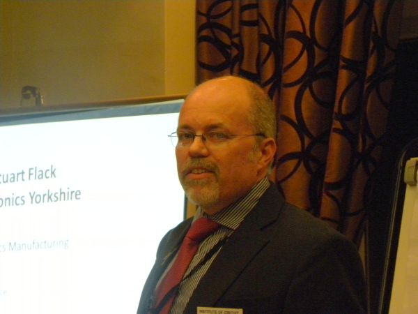 1950s the Institute of Printed Circuits, later the Institute for Interconnecting and Packaging Electronic Circuits, and since 1999 simply IPC (the association connecting electronics industries). With its headquarters in Bannockburn, Illinois, USA, IPC was the electronic industry's leading source for standards and training, supporting programmes to meet the needs of an estimated $2 trillion global electronics industry, with emphasis on design, PCB manufacturing and electronics assembly. IPC was accredited by the American National Standards Institute as a standards-developing organisation, and was a member of the World Electronic Circuits Council.
Flack discussed IPC standards, training and accreditation. Standards defined accepted inter-departmental and inter-company workmanship criteria in a common language, and provided a means to avoid or resolve disputes. There were currently more than 225 active IPC standards, developed by committees of volunteer experts representing the global electronics community. Training and certification provided proof of education in the use of those standards, and in the UK there were currently over 11,000 individual certifications, spread over 800 companies. Furthermore, the IPC accreditation programme provided a traceable system which was simple to verify through the IPC website.
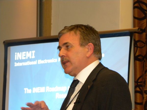 The International Electronics Manufacturing Initiative (iNEMI) is a not-for-profit, R&D consortium of electronics manufacturers, suppliers, associations, government agencies and universities, whose mission is to forecast and accelerate improvements in the electronics manufacturing industry for a sustainable future. Steve Payne, Manager of European Operations, explained how iNEMI's technology roadmap was generated and examined its benefits: assessment of where the industry was at and identification of where wanted to be, comparison of various technology paths and clarification of what was needed to get there, visibility as to what was happening, enhanced communication along the supply chain and defining where collaboration and innovation was necessary.
The iNEMI roadmap gave an outlook for the following 10 years, updated every two years, for the full supply chain for electronics manufacturing, based on the input of over 650 participants from 350 companies and organisations in 18 countries. iNEMI collaborative projects reduced costs by leveraging resources, reduced risks of technology introduction by accelerating the deployment of new technologies, developing industry infrastructure and ensuring reliability and technology readiness when required, as well as reducing environmental risks by ensuring that sustainable solutions were put in place and in step with industry. Current project areas included packaging & component substrates, test, inspection and measurement, environmentally sustainable electronics, optoelectronics, board assembly, organic PCB interconnect, electronic connectors, MEMS and sensors, medical and automotive.
Bill Wilkie brought proceedings to a close, thanking speakers for sharing their knowledge, delegates for their attention and Lamar Group for their generosity in supporting the event. A supper of bacon barm cakes and chip butties was enjoyed by all, and networking continued until late in the evening.
Pete Starkey, I-Connect007, March 2015