Standing Room Only at Winsford.
Institute of Circuit Technology Winsford Seminar. 6th March 2014
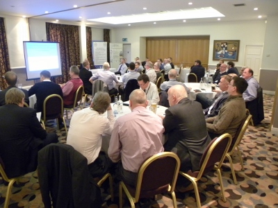
Spring had almost arrived! The snowdrops and crocuses were in flower and buds on the daffodils, but it was a dull and drizzly day in Cheshire UK for the Institute of Circuit Technology Winsford Seminar. The event attracted a sell-out audience and it really was standing-room-only in the seminar room.
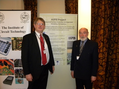
 Technical Director Bill Wilkie introduced a programme of four presentations on a diversity of subjects: bonding treatment, soldering, trace metal removal and semiconductor packaging.
Copper surface preparation to achieve reliable multilayer bonding is a critical operation. In high frequency designs, traditional methods can result in a loss of signal integrity as a consequence of excessive roughening of the copper. Paul Sevriens travelled from MEC Europe in the Netherlands to describe an improved and simplified process of bonding treatment which gave increased peel strength and improved high temperature resistance with minimal surface roughening. A key characteristic of the process was the very low thickness of the copper-organic surface layer, typically 3 nanometres compared with 20 nanometres for competitive processes based on benzotriazole or benzimidazole. This very thin layer did not block the surface texture of the etched copper, and when peel-tested left no residue on the copper. MEC had installations in: Germany, Italy, Switzerland, England, Netherlands, Sweden and USA.
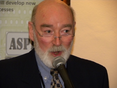
 Dr Andrew Ballantyne had presented at previous ICT seminars, on applications of ionic liquids and deep eutectic solvents in metal finishing. The latest line of research at University of Leicester explored the potential benefits of deep eutectic solvents as replacements for conventional soldering fluxes, and some impressive results had been observed. Compared with conventional fluxes which relied on acidic activators, those based on deep eutectic solvents had the advantages of benign chemistry, low toxicity and environmental impact, low cost, low water sensitivity, high metal solubility and less-onerous registration requirements.
After summarising the chemistry and physical characteristics of ionic liquids in general, and entertaining the audience with a live mix-and-shake demonstration of how easily they could be prepared, Dr Ballantyne reviewed the results of solderability testing on copper, brass, nickel, stainless steel and cast iron. Although the scope of soldering technology clearly extended far beyond the field of electronics assembly, specific testing had been carried out on a range of PCB finishes including bare copper, OSP, ENIG, immersion silver, immersion tin, tin-lead HASL and lead-free HASL, on surface-mount pads, through-holes and BGA pads, all with satisfactory results and all samples passed contamination testing after normal cleaning.
In cooperation with Merlin Circuit Technology, deep eutectic solvent formulations had been evaluated as hot-air solder levelling fluxes with remarkable success. Copper was wetted more rapidly than with proprietary HASL fluxes and complete coverage was achieved in a single dip. One very interesting outcome was the ability to solder-level with lead-free solder on PCBs with electroless nickel finish, not previously achievable with conventional fluxes, and this opened up the prospect of a novel solderable finish dubbed HASLEN – Hot Air Solder Levelling on Electroless Nickel.
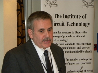
ICT Chairman Professor Martin Goosey gave the third presentation, entitled Recovery of Copper from PCB Manufacturing Processes using Crab Shells, describing the TSB-funded STOWURC project whose objective was to develop sustainable materials and processes using waste products from the seafood industry to treat effluent and recover metals from PCB manufacture.
The whole supply chain, from raw material to dissemination of information, was represented in the project consortium. It had been observed that a natural component of the shells of crustaceans, chitin, was able to adsorb heavy metals from dilute solution, and that a simple chemical modification of chitin, by alkaline deacetylation to form chitosan, significantly improved the efficiency of adsorption. For example, one gram of chitosan was capable of adsorbing 250 milligrams of copper.
Professor Goosey summarised the results of initial experiments. The effects on adsorption rates of parameters such as temperature, pH, initial concentration, rate of mixing, specific metal ions had been studied, over a range of chitosan parameters including the amount of adsorbant, the degree of deacetylation and the particle size. It was possible to reduce copper concentration in effluent to the 0.1ppm level.
Having captured the metal, it was possible to desorb it with sulphuric acid and recover it by straightforward electroplating. A key issue was the residual adsorption efficiency of the chitosan after stripping of copper; there was a tendency for absorption ability to decrease with each cycle, and conditions were being optimised to minimise the effect.
Chitosan had the ability to adsorb a wide range of metals found in PCB effluent, nickel for example, and there were many applications in the general metal finishing industry. It also provided the opportunity to recover endangered or rare metals from low concentration solutions. Professor Goosey mentioned platinum, palladium, rhodium, osmium, iridium, mercury and gold as examples, but made it clear that each metal would need an optimised combination of process parameters and conditions.
 Past Chairman of ICT Steve Payne gave a thought-provoking overview of laminate-based semiconductor packaging and system-in-package technology – effectively an insight into some applications of PCBs in miniature.
With some silicon dies now having as many as 5,500 input-output connections, wire bonding was a not a practicable interconnection option and a flip-chip approach was preferred, with a laminate substrate within the package. This was compatible with BGA-style area-array packaging and gave the electrical benefit of very short interconnects, but mechanically the interconnections were stiff and rigid. Therefore for high reliability applications there was a critical need to match thermal expansion properties of silicon and substrate, and to aim for a low modulus to aid mechanical compliance. Very thin substrates were preferred, to minimise z-axis stresses, and materials without woven-glass reinforcement were favoured, which gave the additional benefits of more efficient laser drilling and the absence of CAF effects.
Typical substrate design rules were 25-35 micron track and gap, to enable conductor routing from flip-chip solder bumps at pitches trending towards 100 microns, 50 micron via holes and 100 micron capture pads, with a construction based on build-up technology having dielectric thicknesses of 40-50 microns. Semiconductor packaging and system-in-package could use the same substrate technology, and there had been heavy investment in Asia to satisfy high volume requirements for smart phones and tablets. The global market for semiconductor packaging materials was expected to grow to over $25 billion by 2015, of which laminate substrates represented the largest market segment, with a growth forecast of 8 percent over the next five years.
Although the manufacture of semiconductor substrates was technically challenging, they were in fact miniature PCBs and Payne indicated that there was a significant and growing requirement for high reliability medium volume substrates in Europe which represented a substantial market opportunity, with typical selling prices in the range £20 - £40 per square inch.
Bill Wilkie brought proceedings to a close, acknowledging the generous support of CC Electronics, and reporting a record number of advance registrations for the ICT/NUKCG Foundation Course in April and a high level of interest in the ICT Annual Symposium and 40th anniversary celebration dinner in June (full details at www.instct.org).
The Institute of Circuit Technology continues to gain momentum, with membership now well into the 300s, and the Winsford Seminar was another excellent opportunity for members to share knowledge and to network with their peers in the UK PCB industry.
Pete Starkey
March 2014