 After an extreme summer heat wave had left trees dehydrated and struggling to morph into their customary display of reds and golds, the leaves were brown and brittle as the great and good of the UK printed circuit board industry crossed the bridge from the mainland of the south coast of England to Hayling Island for the autumn seminar of the Institute of Circuit Technology on September 20, 2018.
ICT technical director Bill Wilkie welcomed delegates to what has of recent years become a highlight of the Institute’s seminar programme and remains an extremely popular event. He emphasised the role of ICT in keeping its membership aware of market trends and emerging technologies, with reference to the demise of some big-name companies who had either failed to recognise those trends or ignored those technologies that had initially appeared to be well-out-of-the-box but had subsequently become mainstream.
He introduced a seminar programme that included a discussion of developments in semi-additive flexible circuit fabrication, an update on global and European market statistics and forecasts, a review of the state-of-the-art in dry film photoresist characteristics and capabilities, and an example of how a good presenter can make potentially dreary legal stuff remarkably interesting.
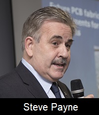 First speaker was ICT vice-chairman Steve Payne, from management and technical consultancy Cirflex Technology, with a presentation entitled “SAP—a Case Study for Flex.”
Payne explained that although the principles of semi-additive processing (SAP) had been established for many years, modified semi-additive processes had become popular in IC substrate production, and were poised for widespread adoption as enabling technologies in the manufacture of ultra-fine-line PCBs, particularly in applications such as the latest smartphones.
The basis of the SAP concept was to use pattern plating to selectively build up the thickness of copper tracks on a very thin base copper, in order to reduce undercut effects when the base copper was etched away. Clearly, the thinner the base copper, the less the undercut, and hence the better the capability to fabricate very fine tracks and gaps.
Payne referred to a case study where semi-additive processing had been employed in the fabrication of flexible circuits with tracks and gaps of 25 microns and less. Obviously, it had been necessary to start with extremely thin base copper, and the choices were to procure flexible materials manufactured with very thin copper foil, to reduce the thickness of standard copper-clad flexible material by controlled etching, or to seek an alternative technique such as sputter-deposition of copper. In Payne’s example, reel-to-reel DC magnetron sputtering had been used to deposit very thin copper onto polyimide film. Because this deposit thickness could be less than one micron, special techniques were demanded in photoimaging and pattern plating processes, but etch undercut was practically eliminated and track and gaps of 25 micron or less could be achieved in good yield. The sputter process could also metallise laser-drilled through-via holes.
Payne discussed the principles of DC magnetron sputtering, described a typical process flow for semi-additive 2-layer flex, and showed examples of flexible circuitry produced using this technology, which was in production in certain locations in the U.S. and the Far East.
 Market analyst and ICT council member Francesca Stern delivered her eagerly-awaited annual review of the global outlook for the PCB and electronics industries. She began with a well-illustrated and authoritative overview of trends in electronics and PCB production in Europe, USA, Japan and China, commenting that there appeared to be a slight slow-down in 2018 as compared with 2017. Consumer electronics production in Germany was definitely moving downwards. It was encouraging that figures for the UK electronics industry were currently looking better than for some other major Western European producers, but growth forecasts for the next two years indicated that the UK would show a downturn later in 2018. The U.S. was currently performing quite well, especially in instrumentation and military areas, but was also expected to show a downturn later in 2018. Japan continued to show negative growth. In China, base stations for 5G were a significant growth area, but so far 2018 had not been a good year for China overall. Global PCB production was valued at around $63 billion in 2017, of which the UK’s share was £128 million with a slight increase to £130 million predicted for 2018.
“Imagine Imaging” was the headline of the third presentation, given by MacDermid Enthone’s John Cornforth, a regular contributor to the ICT foundation course. He described how a relationship had been established between MacDermid Enthone and Hitachi Chemical for the supply of dry film photoresist to the European PCB and metal finishing industries, and discussed the logistics of the supply chain. The products were manufactured in Malaysia and shipped as master rolls to a new cleanroom facility in the UK for slitting to the widths and lengths required by the European market, for which all of the necessary certifications were in place. Cornforth discussed electronics industry trends and the imaging demands of current and emerging PCB manufacturing technologies, an example being semi-additive processing for which thinner resists were required. With reference to Hitachi’s product portfolio, which also included materials for the microelectronics industry, he outlined typical applications for a range of different product types, and reviewed typical customer future requirements which included faster exposure, finer lines, improved adhesion, better tenting and faster stripping. There was a trend for LDI exposure systems to employ shorter wavelengths, and Cornforth described the characteristics of a new dry film specifically developed for 405 nm exposure.
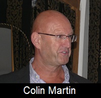 The final presentation, given by Colin Martin of ParaChem Consulting Chemists, was an update on the REACH regulations. He remarked that of the four presentations of the evening his might well be the stinker, especially as it was on the subject of environmental compliance and the range of “interesting work” that this invariably created. REACH, a European Union regulation concerning the Registration, Evaluation, Authorisation & restriction of CHemicals, applied to most businesses in the UK in some way, and was a significant consideration in the PCB industry where it impacted the use of chemicals “from cradle to grave,” both upstream and downstream. Martin gave an introduction to the REACH regulations, and commented that although this was European legislation, the requirements applied to any product sold into the European Union and would continue to apply in the UK after “Brexit.” He discussed the significance of REACH in the PCB industry and explained the meaning of “substances” in “articles,” and the declarations PCB producers were obliged to make to their customers if “Substances of Very High Concern” (SVHCs) were present at more than 0.1% w/w in an “article,” including providing “sufficient information, available to the supplier, to allow safe use of the article including, as a minimum, the name of that substance.” Guidance was available in Article 33 of the REACH regulations.
Specific examples of SVHCs included boric acid, potassium chromate and various organic materials. As of June 2018, further substances had been added including lead, which was still used in some electronics soldering applications. This meant that boards assembled using lead-based solders would need to be weighed to determine if the lead was present at more than 0.1% w/w. Martin commented that HASL-finished boards could well contain more than 0.1% w/w of lead. Compliance statements were necessary for every single product made, so it was important to implement an efficient and systematic approach. ParaChem had developed an online database called ReachWARE, which could assess products and produce compliance reports. Compliance had been a legal requirement since 2009 and failure to make a declaration was a criminal offence, although Martin believed that no-one had so far been prosecuted and, although there was no choice but to comply, there was no need to despair!
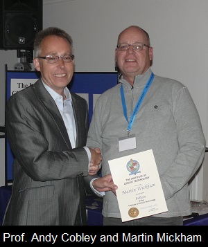
Martin Wickham, well known for his work at the National Physical Laboratory, had recently been elected a Fellow of the Institute and he was presented with his fellowship certificate by ICT chairman Professor Andy Cobley, who then thanked the speakers for sharing their knowledge, and MacDermid Enthone for supporting the event. And special thanks to Bill Wilkie for his diligent organising work behind the scenes, and for chairing the seminar.
I am grateful to Professor Martin Goosey for his assistance in preparing this review.
